background image

CD-C1W,CP-C1W

– 15 –

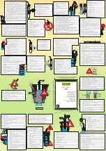
EXPLANATION OF AUTOMATIC SOUND VALUE CORRECTION CONTROL

1. Outline

The recent trend is toward rise of CD record level in the world, for example rock, dancing music, etc. In case of continuous high
level playback G-EQ (graphic equalizer) and VOL (Volume) are controlled (lowered) automatically after a lapse of specific time
(10 minutes) so as to get the easy-to-listen sound level.

2. Explanation of operation

The CD playback operation is explained below.

A

X

B

C

D

0w

10 minutes

Distortion clip point

SP output
level

  X  : Threshold value of control circuit operation
  A  : Hight energy (hatched area) exceeding  X  is detecated, and the control mode is set.
  B  : After a lapse of 10 minutes the control is started.

Data is fetched every 4
seconds to control.

Initial frequency
characteristics.

Hand L frequency char-
acteristics are lowered.

VOL (Volume) is lowered.

At first, the  H and  L frequency characteristics are lowered as shown above so  thet the distortion
and disturbance are reduced. However, if hight energy exceeding  X  is detected, VOL is lowered
to get sound easy to listen.

Stable control
Continued control

The output data is fetched every  4 seconds  to  control. When quiet music is played back, the
control is performed so as to restore the initial frequency characteristics and initial VOL values.

Control mode cancel conditions

When output exceeding   X   is not given
continuously for 10 minutes.

When quiet music is played back.
When VOL is lowered.

When the power is turned off or on.

B  ~  C  :

C  ~  D  :

Содержание CD-C1W

Страница 1: ...ANUAL SHARP CORPORATION No YS792CDC1W In the interests of user safety the set should be restored to its original condition and only parts identical to those specified should be used This document has been published to be used for after sales service only The contents are subject to change without notice SRS technology Licensed from SRS Labs SRS technol ogy holds the following patents U S Patent No...

Страница 2: ... LEVEL OF THE LASER POWER OUTPUT IS LESS THAN CLASS 1 BUT THE LASER COMPONENT IS CAPABLE OF EMITTING RADIATION EXCEEDING THE LIMIT FOR CLASS 1 THEREFORE IT IS IMPORTANT THAT THE FOLLOWING PRECAUTIONS ARE OBSERVED DURING SERVICING TO PROTECT YOUR EYES AGAINST EXPOSURE TO THE LASER BEAM 1 WHEN THE CABINET IS REMOVED THE POWER IS TURNED ON WITDOUT A COMPACT DISC IN POSITION AND THE PICK UP IS ON THE ...

Страница 3: ...r D A converter 1 bit D A converter Frequency response 20 20 000 Hz Dynamic range 90 dB 1 kHz Wow and flutter Unmeasurable less than 0 001 W peak Tuner section Frequency range FM 88 108 MHz SW2 9 5 21 85 MHz SW1 3 2 7 3 MHz MW 531 1 602 kHz Cassette deck section Type Compact cassette tape Frequency response 50 14 000 Hz Normal tape 50 15 000 Hz CrO2 tape Motor DC motor with electronic governor 1 S...

Страница 4: ...7 TAPE Dolby NR Indicator 28 TAPE Reverse Mode Indicator 29 TAPE Record Indicator 30 CD Play Indicator 31 CD Repeat Indicator 32 Spectrum Analyzer Volume Level Indicator 33 FM Stereo Indicator 34 FM Stereo Mode Indicator 35 CD Clear Button 36 Memory Set Button 37 TAPE Reverse Mode Button 38 TAPE Reverse Play Button 39 TUNER Tuning Down Button 3 CD Track Down Review Button 3 TAPE Fast Wind Button 4...

Страница 5: ...ton 13 Track Up Cue Button 14 CD Select Direct Play Buttons 15 Play Repeat Button 16 Stop Button 17 Memory Button 18 Clear Button 19 Random Button 10 Pause Button Tuner control section 11 Preset Up Down Buttons Tape control section 12 Reverse Play Button 13 Record Pause Button 14 Stop Button 15 Forward Play Button 16 Fast Wind Buttons Common section 17 3D Surround Pass Button 18 3D Surround Mode B...

Страница 6: ... 1 minute Keep turning the dial to advance continuously The hour setting will not advance even if minutes advance from 59 to 00 9 Press the MEMORY SET button The clock starts operating from 0 seconds Seconds are not displayed Note In the event of a power failure or when the AC power lead is disconnected the clock display will go out When the AC power supply is restored the clock display will flash...

Страница 7: ...anel to MW tuning interval span of your area To change the tuning zone 1 Press the ON STAND BY button to enter the stand by mode 2 Set the SPAN SELECTOR switch to 50 9 for 9 kHz MW interval 50 kHz FM interval and 100 10 for 10 kHz MW interval 100 kHz FM interval 3 Press and hold down the button the EQ DEMO button and the ON STAND BY button all at the same time Hold them for at least 1 second Cauti...

Страница 8: ...ntioned notes when disassembling the unit and reassembling it to keep it safe and ensure excellent performance 1 Take cassette tape and compact disc out of the unit 2 Be sure to remove the power supply plug from the wall outlet before starting to disassemble the unit 3 Take off nylon bands or wire holders where they need be removed when disassembling the unit After servicing the unit be sure to re...

Страница 9: ... E1 x2 E4 x1 Ø3x10mm E3 x2 Display PWB Main PWB Front Panel Pull Power PWB F1 x1 D1 x8 Ø3x10mm Power AMP PWB D3 x4 Ø3x10mm F2 x1 Ø3x6mm E5 x1 Ø3x8mm Tuner PWB F1 x1 Lug Wire F3 x2 Ø3x10mm Rear Panel H1 x3 Ø3x10mm G3 x12 Ø3x10mm K1 x6 Ø3x10mm Lug Wire J1 x1 Ø3x8mm Open Headphones PWB Display PWB G1 x2 G2 x1 Washer Tape Mechanism Cassette Holder Left Right Front Panel CD Switch PWB L3 x1 Ø3x6mm M1 x...

Страница 10: ...sc trays 1 2 and 3 turn over the mechanism unit push two pawls and remove successively the three disc trays from the mechanism unit starting with the disc tray 3 Thereby the CD mechanism shown in the right figure can be removed R1 x2 ø2 x7mm R5 x1 ø2 6 x12mm R10 x4 ø2 6 x10mm R3 x1 R2 x1 R6 x1 R9 x1 Disc Tray 2 Disc Tray 3 Spring R4 x3 1 2 3 Normal state Press in turns the arrow parts starting wit...

Страница 11: ... Fig 11 4 1 Remove the Top cabinet 2 Disassemble as shown in the figure so that the CD disc of CD changer can be taken out 3 Remove the CD disc from the tray as shown in the figure How to remove the CD disc When CD is in playback state See Fig 11 3 1 Remove the Top cabinet 2 Disassemble as shown in the figure so that the CD disc of CD changer becomes visible 3 Remove the CD disc as shown in the fi...

Страница 12: ...ection L VR101 Normal 45 10 mV L TP490 4 R VR102 CrO2 65 15 mV R TP490 2 Adjusting Point Specified Value Tape 1 Playback Amplifier Sensitivity Adjusting Point Instrument Connection L VRD01 L TP451 3 R VRD02 R TP451 1 Test Tape Specified Value MTT 150 Normal 300 mV Tape 2 Playback Amplifier Sensitivity Adjusting Point Instrument Connection L VRD03 L TP451 3 R VRD04 R TP451 1 Test Tape Specified Val...

Страница 13: ...button pressed turn on POWER Then the frequency is initially set in the memory as shown in Table Call it with the PRESET button to use it for adjustment and check of tuner circuit Preset No 1 87 50 MHz 6 531 kHz 11 3 2 MHz 16 9 5 MHz 2 108 00 MHz 7 1 602 kHz 12 7 3 MHz 17 21 85MHz 3 90 00 MHz 8 603 kHz 13 3 9 MHz 18 11 65 MHz 4 106 00 MHz 9 1 404 kHz 14 7 1 MHz 19 21 45 MHz 5 98 00 MHz 10 990 kHz ...

Страница 14: ...ing servo is acti vated playback will begin at the current position Press the STOP button The pickup willreturn to the STOP position MEMORY key input When the track ing servo is acti vated playback will begin at the current position STOP key input The pickup nor mally returns to the STOP posi tion MEMORY key input IL is not performed Press STOP key Stop TOC IL is performed and the ordinary PLAY is...

Страница 15: ...ode is set B After a lapse of 10 minutes the control is started Data is fetched every 4 seconds to control Initial frequency characteristics Hand L frequency char acteristics are lowered VOL Volume is lowered At first the H and L frequency characteristics are lowered as shown above so thet the distortion and disturbance are reduced However if hight energy exceeding X is detected VOL is lowered to ...

Страница 16: ...he unit of capacitor a symbol P is used this symbol P means micro micro farad and the unit of the capacitor without such a symbol is microfarad As to electro lytic capacitor the expression capacitance withstand volt age is used CH TH RH UJ Temperature compensation ML Mylar type P P Polypropylene type Schematic diagram and Wiring Side of P W Board for this model are subject to change for improvemen...

Страница 17: ...CONTROL CE SL SL DRF 7 3 5V 62 64 56 45 36 23 43 37 38 39 28 25 24 27 26 40 61 58 53 10 12 20 32 40 43 44 53 52 51 54 31 30 29 23 27 16 15 41 44 Q1 5V Q81 7 3V B2 VOLTAGE REGURATOR SWITCHING DRIVER IC82 TA7291S TRAY MOTOR DRIVER XOUT EFMO EFMIN CLV JP RCHO RVSS LVSS LCHO VVDD VDD LVDD RVDD XVDD CONT3 CONT1 CONT2 CONT4 CONT5 TO MAIN SECTION 6 2 8 1 9 5 IC81 TA7291S MAIN CAM MOTOR DRIVER 7 3 CAM SWI...

Страница 18: ...MW B T307 T308 T303 T304 SW1 SW2 OSC SW1 SW2 ANT T306 MW OSC T302 MW ANT B7 AMP LT02 FM RF LT01 FM OSC ICT01 TA7358AP FM FRONT END TT01 FM IF CF302 FM IF BIAS AJDUST VR101 VR102 HI SPEED SOL1 2 SOLENOID SWE1 TAPE1 PLAY SWE7 SWE8 TAPE2 SIDE A FP SIDE B FP SWE5 TAPE2 CrO2 SWE2 TAPE1 CrO2 MOTOR DRIVER QM02 QM01 QM08 QM03 QM04 T2 PLAY T1 PLAY PHM1 PHM2 DRIVER TAPE MOTOR HI SPEED PB EQ HI SPEED NOR HI ...

Страница 19: ...1 AC T F POWER TRANSFORMER Q905 Q906 4 6V ICP01 NJM4565M BUFFER AMP SRS PASS Q463 Q465 Q466 467 Q464 B8 B6 B8 VOLTAGE REGURATER SRS A SRS B SRS IN H PASS SRS STEREO SRS MONO SRS PASS 3D L R C451 S5250AS SRS DOLBY ON OFF DOLBY PL REC PB MUTE REC MUTE T1 T2 T2 B FP T2 CrO T2 RUN T2 PLAY STOP T2 A FP T2 SOLENOID HIGH SPEED T1 PLAY STOP T1 RUN T1 CrO T1 SOLENOID TAPE MOTOR CD MUTE CE CL DI CCB DO CCB ...

Страница 20: ...0 C532 C522 C524 C540 C534 C516 C518 C536 C510 C546 C508 C504 C506 C507 C545 C535 C509 C517 C579 C521 C515 CT05 Q821 C825 C821 Q827 F820 T500mA L 250V CD02 CT18 CT17 CT09 QT01 CD14 CD13 CD12 R827 ZD821 R834 R826 R820 R460 ZD452 ZD451 R467 R477 C831 RD21 D403 D829 R515 R509 R511 R510 RT18 R948 R947 CD06 RD15 R592 R591 R RD75 RD37 R941 RP15 RP16 ZD820 R470 RP14 RD71 RD27 DD02 RP13 R942 RP09 RP10 RP3...

Страница 21: ...3 C131 C128 C141 C109 Q108 VR102 CD35 CD36 CD13 CD12 R163 R148 RD73 R107 R109 R221 D206 D401 RM06 R467 C208 DM03 RD38 D402 R185 R141 RA87 RA88 R224 R225 R226 R227 R228 R223 R201 D554 RA74 R112 RD72 RD76 RD69 DD01 R153 R137 R135 RD37 R161 R160 R166 RA76 ZD201 R207 RA77 DM02 RM10 RM12 RM04 RM11 R119 RD71 R133 R158 D27 RD44 R583 R553 R582 ZD550 R211 D203 L201 RA81 R208 R202 R595 R210 RA08 RA09 RA07 R...

Страница 22: ...3V CD 7 3V CD PCCC GND 4A CQCK COIN SQ_OUT TRY_SW4 TRY_SW3 WRQ DRF PIUN TRY_SW2 TRY_SW1 CAM_SW4 CAM_SW3 CAM_SW2 CAM_SW1 RWC SL SL RES GND CD2 GND D PCCL RWC SL SL RES AUT_SCAN VOL SW MOTOR SP DET POSISTOR PROTECT TUN_SM SP_16K SP_4K SP_1K T1_CROM T2_A FP T1_RUN BEAT_CUT TA_BIAS T2_B FP T2_CROM T2_RUN T2_PLAY T2_SOL T1_SOL T1_PLAY HIGH_SP TA_R P TA_PB EQ SRS_A NA DOL_A NA DRF CD_MUTE CQCK SQ_OUT CO...

Страница 23: ... C2B_DI C2B_CE C2B_DO TUN_MUT TUN_SD TUN_SM RESET POINT PROTECT 4 6V D LINE MUTE VOL SW SP DET POSISTOR S MUTE FUN CONT SP PROT SP RELAY POWER H P SW GND D3 15V 12V A 12V M 7 3V CD GND D CD GND D1 CD GND D2 4 6V D 12V M GND D 7 3V CD CD GND D1 CD GND D2 4 6V GND µ CON 4 6V µ CON REC EQ REC_MUT TA_T1 T2 PASS SRS PASS 15V SRS INH SRS B SRS A OUT R OUT L IN L IN R 12V A GND A TO AMP SECTION P26 3 H V...

Страница 24: ...0 VRD01 22K B CD52 1 50 RD72 6 8K 22K B VRD02 QD07 KRC107 M CD51 1 50 RD71 6 8K QD06 C104M CD14 10 16 RD12 10K RD13 10K RD03 1K RD14 10K CD13 0 22 50 RD11 10K CD17 10 16 RD01 1K CD01 1 50 R134 68K QD10 KRC107 M QD09 KRC107 M VRD04 22K B VRD03 22K B CD02 1 50 RD02 1K ICD01 1 2 HA12134A DOLBY NR RD10 10K CD04 470P CD03 470P CD12 0 22 50 CD18 10 16 R133 22K Q140 KRC104 M R180 5 6K R128 5 6K Q114 KRC1...

Страница 25: ... 1 50 RD31 8 2K CD39 0 1 50 RD29 1 2K RD36 100 RD34 5 6K RD33 5 6K RD27 68K CD43 0 022 CD44 0 022 RD30 1 2K CD38 10 16 RD35 1M CD41 22 25 CD37 10 16 CD20 150P CD14 10 16 RD12 10K RD13 10K RD22 68K RD21 68K RD14 10K RD11 10K CD17 10 16 RD10 10K 2 50 CD19 150P CD18 10 16 3 1 2 13 21 25 18 17 19 20 14 15 26 27 31 29 28 30 23 24 16 BEAT CUT TA_PB EQ H NORM L CrO2 T2 CRO BIAS UT LO L HI H T B H REC L C...

Страница 26: ... 27K CP13 10 16 CP14 10 16 RP16 220 RP37 68K CP11 100P RP07 1K RP05 2 2K RP09 10K QP01 KTC3199 GR R947 12K ICP01 1 2 68K RP38 CP12 100P RP08 1K RP10 10K R948 12K QP02 KTC3199 GR 67 68 69 62 72 71 70 42 78 79 80 470 CrO2 SOL NC COM SENSOR OUT 5V SENSOR PLAY SW MOTOR SPEED A MOTOR SPEED B NC R_REC F_REC CrO2 SOL SENSOR OUT 5V SENSOR PLAY SW COM MTR SENSOR OUT 5V SENSOR PLAY SW CrO2 SOL NC COM NC R_R...

Страница 27: ... 50 4 3 2 1 14 13 12 11 10 9 8 7 6 5 4 3 2 1 11 2 10 4 SOL MTR 12V M HIGH_SP SOL CrO2 SENSOR OUT CrO2 SENSOR OUT GND M PLAY SW R_REC F_REC PLAY SW 4 6V D R CH L CH GND R CH L CH VOL SW SP DET 12V M GND M H P SW POSISTOR RELAY PROT FAN CONT 15V GND A FW903 1 1 14 14 CD GND D GND M 12V A SP DET POSISTOR H P SW RELAY FAN CONT PROT 15V VOL SW POWER POSISTOR SP DET 15V GND D 12V A 12V M RELAY PROT S MU...

Страница 28: ...7 270 R477 270 C488 0 022 C487 47 25 ZD452 MTZJ8 2C Q463 KRC107 M R470 10K R474 10K R473 10K Q464 KRC107 M C453 2 2 50 C471 100 16 R471 100K R472 100K 56 57 58 59 60 61 62 55 63 64 65 17 6 28 27 26 25 24 23 22 21 20 19 18 16 15 13 11 14 12 10 9 8 7 5 4 3 2 1 5 3 6 9 12 10 13 4 8 11 7 14 2 1 0V 0V 0V 0V 2 6V 0V 0V 0V 0V 0V 0V 8 3V 0V 0V 1 6V 0V 1 6V 0V 0V 8 3V 8 3V 8 3V 0V 0V 0V 0V 0V 2 6V 11 7V 11...

Страница 29: ... C383 TO MAIN PWB C382 C387 C380 R376 R360 R397 R398 RT09A QT01A CT16A CT15A CT11A CT02 CT01 BFT01 CT08A RT02 R310 D305 D301 D309 D311 D303 D307 C331 R319 D312 T306 C334 C335 TC304 TC305 T307 R325 L353 C349 T308 Q307 Q308 T302 D308 R320 R318 L311 D304 D302 D306 CT09A CT03A CT05A CT10A CT06 C304 C305 C 3 3 0 C338 C306 C309 C314 R317 R314 R313 C307 C313 C321 C320 R342 R326 R330 R329 VR351 R343 R315 ...

Страница 30: ...328 10K C318 0 022 R322 5 6K C316 0 1 R320 10K R318 1 5K R324 100K R319 100K C331 0 047 VD301 1 KV1236Z23F C342 0 022 VR351 10K B R382 150 X352 4 5MHz D304 1SS133 D303 1SS133 R321 5 6K 1SS133 D312 C315 0 1 VD301 2 KV1236Z23F C336 470P R323 68K R327 5 6K Q307 2SC2878 B TC304 Q306 2SC2878 B TC305 RT09A 820 C381 12P C C382 15P C L356 1mH R341 47K Q364 KRA107 M Q362 KRA107 M Q363 KRA107 M R342 47K R34...

Страница 31: ...12P CH C382 15P CH L356 1mH R395 47K C386 330P R341 47K Q362 KRA107 M C351 0 022 R351 5 6K 2 06V 0V 12 18V 5 01V 2 07V 2 06V 0V 0 65V 0 65V 11 6V 12 18V 11 37V 0V 0V 0V 0V 2 52V 2 52V 0V 0V 0V 4 82V 5 1V 0 16V 12 1V 3 85V 3 95V 5 1V 2 38V 0V 0V 0V 2 48V 5 11V 0 9V 0 9V 2 1V 0V 5 09V 5 09V 2 84V 5 01V 3 68V 3 85V 3 85V 3 95V 1 18V 1 19V 2 05V 2 29V 2 52V 0V 0 46V 2 2V 2 2V 5 01V 3 48V C352 10 16 L3...

Страница 32: ...705 Q704 R707 Q703 Q702 R784 R706 R724 RY41 RY40 R703 R702 R701 SW723 SW721 CLOCK SW722 SLEEP TIMER SW713 C710 C711 LED714 LED708 LED707 LED701 LED702 LED703 LED705 C728 C729 C730 C702 X701 LED717 LED716 LED718 SW719 LED715 LED725 SW708 STOP SW718 CD PAUSE SW733 MEMORY SET SW732 CLEAR SW734 POWER ON STAND BY SW725 SW724 LED724 LED726 LED709 SW707 F F SW717 REWIND SW720 REVERSE PLAY REVERSE MODE SW...

Страница 33: ...C37 R60 C38 R55 R66 R64 R36 R46 R1 C2 R12 R9 R8 R10 C54 R31 R71 R72 R56 C23 R40 C24 R22 R24 R23 R18 R17 R73 C74 R34 R48 C73 R74 R2 R5 R4 R3 R7 R6 R33 R32 R30 R35 C16 R28 R29 C17 C21 R25 C14 R16 R14 R13 R52 R53 R44 R50 C83 C53 C56 R39 R42 R38 R43 C25 R45 C32 R27 R21 C13 R26 C10 R15 R80 R81 R82 C80 R85 R87 R86 C85 5V 4 8 3 2 6 4 3 3 1 7 1 6 1 1 6 4 4 8 4 9 3 2 3 3 1 7 1 6 Q51 C55 C6 C5 C9 C8 C11 C12...

Страница 34: ...LOF FSTA TOSTA FOSTA 8 12CM LASER 2FREQ RF REF REF REF REF TO REF REF REF REF VCR VCR VCR TGL1 THDL GL THD VCC DRF S Q R PSTR REF TO VCC1 SPI JP SPG SP SPO FD FA FA SP THLD TD TD TO TA TH TE TE TB F E FIN1 FIN2 LDS LDO BHI PHI LF2 SLI VR REFI VCC2 DRF CE DAT CL CLK DEF DGND SLC RFS RFSM CV CV SLOF HFL TES TOFF TGL JP FE FE FD AGND SLEO SLD SL SL JP FSC NC VCC CH1 CH2 CH4 CH3 TSD STAND BY IC3 M5674...

Страница 35: ...3 PDO VSS 4M 16M TST11 DOUT C2F EMPH FSEQ PCK FSX RES CQCK COIN SQOUT RWC WRQ SBCK SFSY PW MUTEL LVDD RVDD MUTER RCHO RVSS LCHO CONT5 CONT4 CONT1 CONT3 CONT2 FR JP JP TGL TOFF CLV CLV V P HFL TES VDD VVDD ISET VVSS TEST4 TEST5 CS 2K x8BIT RAM HF GND CD1 GND D TRY_SW4 TRY_SW3 TRY_SW2 TRY_SW1 CAM_SW4 CAM_SW3 CAM_SW2 CAM_SW1 COIN WRQ CQCK SQ_OUT RWC SL SL RES PCCL 7 3V CD GND CD2 7 3V CD 9 8 7 6 5 4 ...

Страница 36: ...8 7 6 5 4 3 2 1 3 1 2 1 F1 0 4V 0 5V 11 4V 0 5V 11 5V 11 5V 0 5V 0 5V 11 4V 0 4V 0 7V 0 7V 2 0V 3 8V 0V 0V 0 6V 0 6V 0 6V 0 6V 0V 4 0V 32 5V 36 5V 36 6V 32 5V 0 5V 0 5V 0 5V 0 5V 0V SCK1 SO0 SI0 SCK0 SO1 P16 SI1 INT0 P37 P36 P35 P34 P33 P32 P31 P30 P17 CD ON TUNER PAUSE REW REV CD S47 S43 S44 S45 S46 PG0 PG1 PG2 PG3 P00 P01 P02 P03 VSS2 VDD2 P04 P05 P06 P07 S38 S39 VDD4 S40 S41 S42 32 5V 32 5V 4 0...

Страница 37: ...8 S39 VDD4 S40 S41 S42 S25 S24 S23 S22 S21 S20 36 9V 27 4V 36 4V 0V 28 2V 28 2V 28 4V 12 2V 16 0V 32 1V 32 1V 36 4V 36 4V 32 2V 36 6V 36 6V 36 6V 36 6V 32 5V 32 5V 32 5V 4 0V 32 5V 32 5V 32 6V 32 4V 32 5V VP VDD3 S7 S8 S9 S10 S11 S12 S13 S14 S15 S16 S17 S18 S19 6G 7G IC701 IX0206AW FL DRIVER CONTROLLER 10G 1G 2 9V 2 9V 2 9V 2 9V 2 9V 2 9V 2 9V 2 9V 2 9V 2 9V 33 1V 19 8V 19 8V 28 1V 36 4V 4 0V 36 4...

Страница 38: ...1 R907 C909 C910 R908 C914 R912 R911 C913 R909 R910 C912 C911 R995 R973 R998 R977 R974 R967 R988 R987 R915 R916 R968 R979 Q998 C984 C983 Q995 Q994 C988 Q905 C907 C908 Q904 C917 Q903 C918 Q999 C989 C990 C997 Q997 C970 C923 C921 C924 C922 C936 Q906 C935 R975 D993 ZD904 D995 R976 D997 D996 R972 R969 R970 R940 D901 D902 R919 R939 ZD999 D907 D908 R997 R996 D998 ZD901 R991 D999 R928 R927 R925 R926 R990 ...

Страница 39: ...7 267 P21 12 H R851 T2A L 250V BROWN BLUE F855 T2 5A L 250V T2 5A L 250V T5A L 250V F854 F856 T5A L 250V T5A L 250V F858 F857 F853 C853 C866 C857 C855 C851 C865 C852 C856 C868 C867 C854 D859 L851 D870 D853 D854 D852 D855 ZD854 D861 D860 R857 ZD851 ZD853 D858 ZD852 C859 C861 WT853 BI851 FW904 Q851 D851 RL851 D850 C860 C858 8 1 AC POWER SUPPLY CORD 253 AC110 127 220 230 240V 50 60Hz 1 2 3 1 4 1 3 FW...

Страница 40: ...0 1 5K R939 1 5K R925 56K R916 1K R915 1K R913 270 R912 56K R911 56K R908 56K D909 1SS133 D910 1SS133 C923 0 1 ML C924 0 1 ML C914 15P C913 15P C912 47P C911 47P ZD901 MTZJ15A C989 220 25 R909 1K C907 2 2 50 C990 0 022 L902 0 29µH L901 0 29µH C997 47 50 R998 56K R926 56K D902 1SS133 R920 2 2K C936 47 50 R914 270 C935 47 50 D998 1SS133 D901 1SS133 R919 2 2K IC901 1 2 STK41713 POWER AMP 9 8 7 6 5 14...

Страница 41: ...D F853 T2A L 250V C854 0 047 ML C853 0 047 ML C855 47 50 C856 47 50 ZD851 MTZJ30C R934 560 R933 560 ZD998 MTZJ5 1B R978 100K R977 10K C988 10 50 D997 1SS133 D996 1SS133 R976 47 Q999 KTC3199 GR C923 0 1 ML C924 0 1 ML C970 47 25 R974 3 9K R971 22K R973 3 9K R972 22K R996 47K R997 3 3K D999 1SS133 D912 1SS133 D911 1SS133 RL901 RELAY SO901 SPEAKER TERMINALS Q994 KTA1270 Y ZD999 MTZJ6 2B R975 3 9K Q99...

Страница 42: ...V JP CUE 50ms 10 0 V JP 50ms 0 50 V JP 50ms 1 00 V TE 6 7 8 9 0 5ms 10 0 V JP 0 5ms 10 0 V JP 0 5ms 0 50 V JP 0 5ms 1 00 V TE 6 7 8 9 REVIEW 50ms 10 0 V JP 50ms 10 0 V JP 50ms 0 50 V JP 50ms 1 00 V TE 6 7 8 9 PLAY 20ms 1 00 V SPO NORMAL DISC TN0 01 20ms 2 00 V CLV 10 11 PLAY TCD 712 140mm TN0 01 50ms 1 00 V SPO 50ms 2 00 V CLV 10 11 PLAY TCD 712 5s 100mV SLD 1 12 0 5s 100mV SLD 1 12 0 5ms 10 0 V J...

Страница 43: ...hanism cam switch SWB101 to SWB104 and tray switch SWB105 to SWB108 Yes Yes Check the connection between IC201 and SW No ICheck whether output of pins 3 and 7 of main cam motor driver IC81 is normal Check the connection from IC2 to IC81 No Yes Check whether the output of pins 3 and 7 of tray motor driver IC82 is normal Yes Check the motors MOB1 and MOB2 No Check the connection from IC2 to IC82 Che...

Страница 44: ...Waveform is unstable Figure 44 2 Figure 44 3 The CD operation keys work Check the FOCUS HF system Playback can be performed without a disc Does the pickup move up and down two twice Yes No Focus search OK Check 4 MHz of IC1 pin 50 CLK line and the microcomputer data of pin 51 CL pin 52 DAT and pin 53 CE Yes Does the output waveform of IC1 pin 16 FD match that shown in Figure 44 1 Yes No Check the ...

Страница 45: ...Playbackisimpossible although initialization is possible Yes Yes Check the periphery of IC1 pin 14 Figure 45 1 3 4 5ms 1 00 V IC1 7 TE 5 ms 5 0 V IC1 54 DRF Check the spindle system Yes Yes Play operation is performed without disc The turntable rotates a little The turntable fails to rotate or rotates at high speed The spindle driver is normal No Checking the VCO PLL system Play operation is perfo...

Страница 46: ...ier input 25 SPG Pin to connect gain setting resistor in the 12cm mode of spindle 26 SP Pin to connect spindle phase compensation constant together with SPD pin 27 SPO Spindle control signal output pin 28 SLEO Pin to connect thread phase compensation constant 29 SLD Thread control signal output pin 30 SL Input pin of thread feed signal from micro computer 31 SL Input pin of thread feed signal from...

Страница 47: ...acitor for peak hold of RF signal 61 BHI Pin to connect capacitor for bottom hold of RF signal 62 LDD APC circuit output pin 63 LDS APC circuit output pin 64 VCC1 RF system VCC pin Figure 47 BLOCK DIAGRAM OF IC IC1 VHiLA9241M 1 Servo Amp LA9241M 2 2 1 FIN2 FIN1 E F TB TE TE TESI SCI TH TA TD TD JP TO FD FD FA FE JP TGL TOFF TES HFL SLOF CV CV RFSM RFS SLC SLI DGND FSC TBC NC DEF CLK CL DAT CE DRF ...

Страница 48: ...nal synchronous signal detection H is output when synchronous signal detected by EFM signal matches synchronous signal internally generated 23 VDD Power terminal of digital system 24 CONT1 Output OPEN direction 25 CONT2 Output CLOSE direction 26 CONT3 Output Cam motor forward rotation 27 CONT4 Output Cam motor reverse rotation 28 CONT5 Output Cam motor speed selection High speed L Low speed H 29 E...

Страница 49: ... 0when not controlled 64 TEST1 Input Input terminal for test Pull down resistor is integrated Surely connected to 0V Pin No Note The same potential must be supplied to the power terminals VDD VVDD LVDD RVDD XVDD In this unit the terminal with asterisk mark is open terminal which is not connected to the outside Figure 49 BLOCK DIAGRAM OF IC IC2 VHiLC78623K 1 Servo Signal Control LC78623K 2 2 IC2 VH...

Страница 50: ...t PROTECT mode 29 INT3 Input 30 PA0 B FP SW Input Tape B FPSW 31 PA1 A FP SW Input Tape A FP SW 32 PA2 T2 CrO SW Input Tape T2 CrO SW 33 PA3 T1 CrO SW Input Tape T1 CrO SW 34 PA4 T2 RUN Input Tape T2 RUN pulse 35 PA5 T2 PLAY SW Inputt Tape T2 PLAY SW 36 PA6 Voltage selection Output Voltage selection 37 PA7 MOTOR Output Tape motor output 38 PB0 T2 SOL Output For tape T2 sol drive 39 PB1 T1 SOL Outp...

Страница 51: ...r Amp MUT signal 78 PF6 S W MUT Output Superwoofer Amp MUT signal 79 PF7 POWER Output Set power control ON H OFF L 80 PL6 9K 10K Input Span selection 9K H 10K L 81 PL5 MIC provided not provided Input MIC existence nonexistence detection Existence L Nonexistenece H 82 PL4 Input 83 PL0 H P SW Input H P existence nonexistence detection 84 PL1 AUT provided not provided Input Tuner AUT scan function pr...

Страница 52: ...n in the internal latch with a timing of changing H to L and the specific analog switch is actuated Data transfer is enabled on the H level 26 VSS GND 27 LVREF Internal analog ground terminal 28 LROUT Output terminal of Lch rear side control 29 LRCOM Common terminal of Lch rear side 1dB step control 30 LRIN Input terminal of Lch rear side 4dB step control 31 LFOUT Output terminal of Lch front side...

Страница 53: ...AN7 KEY6 Input Button input 46 to 54 27 P71 INT1 MAL_UP Input Multi Button jog input UP 28 P72 INT2 T0IN MAL_DOW Input Multi jog input DOWN 29 P73 INT3 T0IN REM_IN Input Remote controller input 30 S0 T0 G15 Output Display tube grid drive 31 S1 T1 G14 Output Display tube grid drive 32 S2 T2 G13 Output Display tube grid drive 33 S3 T3 G12 Output Display tube grid drive 34 S4 T4 G12 Output Display tu...

Страница 54: ...tube segment drive 75 S42 PF2 S1 Output Display tube segment drive 76 S43 PF3 Output NC 77 S44 PF4 LED1 Output LED output H Lights Not defined 78 S45 PF5 LED2 Output LED output H Lights Not defined 79 S46 PF6 LED3 Output LED output H Lights F PLAY 80 S46 PF7 LED4 Output LED output H Lights STOP 81 S48 PG0 LED5 Output LED output H Lights FF 82 S49 PG1 LED6 Output LED output H Lights REW 83 S50 PG2 ...

Страница 55: ...39 S40 S41 G1 S21 S22 S23 S24 S25 S26 S27 S28 S29 S30 S31 S32 S33 S34 S35 S36 S37 S38 S39 S40 S41 G2 S21 S22 S23 S24 S25 S26 S27 S28 S29 S30 S31 S32 S33 S34 S35 S36 S37 S38 S39 S40 S41 G3 S21 S22 S23 S24 S25 S26 S27 S28 S29 S30 S31 S32 S33 S34 S35 S36 S37 S38 S39 S40 S41 G4 S21 S22 S23 S24 S25 S26 S27 S28 S29 S30 S31 S32 S33 S34 S35 S36 S37 S38 S39 S40 S41 G5 S21 S22 S23 S24 S25 S26 S27 S28 S29 S3...

Страница 56: ...CD C1W CP C1W 56 MEMO ...

Страница 57: ...tor type VC MF Cylindrical type without lead wire VC MN Cylindrical type without lead wire VC TV Square type without lead wire VC TQ Square type without lead wire VC CY Square type without lead wire VC CZ Square type without lead wire VC J The 13th character represents capacity difference J 5 K 10 M 20 N 30 C 0 25 pF D 0 5 pF Z 80 20 If there are no indications for the electrolytic capacitors erro...

Страница 58: ...5 1 J AF Silicon PNP 2SB1375 Q903 904 VSKTC3200GR 1 J AC Silicon NPN KTC3200 GR Q905 906 VSKTC3199GR 1 J AB Silicon NPN KTC3199 GR Q994 VSKTA1270Y 1 J AD Silicon PNP KTA1270 Y Q995 VSKTC3199GR 1 J AB Silicon NPN KTC3199 GR Q997 999 VSKTC3199GR 1 J AB Silicon NPN KTC3199 GR QD01 02 VS2SC2878A 1 J AE Silicon NPN 2SC2878 A QD03 VSKRC107M 1 J AC Digital NPN KRC107 M QD06 VSKRC104M 1 J AC Digital NPN K...

Страница 59: ...VCTYPA1CX104K J AB 0 1 µF 16V C13 VCKYMN1HB331K J AA 330 pF 50V C14 VCTYMN1CY103K J AA 0 01 µF 16V C16 VCTYMN1CX472K J AA 0 0047 µF 16V C17 VCKYMN1HB102K J AA 0 001 µF 50V C18 RC GZA474AF1H J AA 0 47 µF 50V Electrolytic C19 RC GZA105AF1H J AB 1 µF 50V Electrolytic C20 RC GZA476AF1A J AB 47 µF 10V Electrolytic C21 VCTYMN1CX332K J AA 0 0033 µF 16V C22 VCCSPA1HL221J J AA 220 pF 50V C23 VCTYMN1CX272K ...

Страница 60: ...rolytic C509 510 RC GZA106AF1H J AB 10 µF 50V Electrolytic C511 512 VCKYMN1HB101K J AA 100 pF 50V C515 516 RC GZA474AF1H J AA 0 47 µF 50V Electrolytic C517 518 RC QZA184AFYJ J AC 0 18 µF 50V Mylar C521 522 RC GZA224AF1H J AA 0 22 µF 50V Electrolytic C523 524 RC QZA124AFYJ J AC 0 12 µF 50V Mylar C525 526 RC GZA224AF1H J AA 0 22 µF 50V Electrolytic C527 528 RC QZA273AFYJ J AB 0 027 µF 50V Mylar C529...

Страница 61: ...29 VRD MN2BD563J J AA 56 kohms 1 8W R30 VRD MN2BD682J J AA 6 8 kohms 1 8W R31 VRD MN2BD122J J AA 1 2 kohms 1 8W R32 VRD MN2BD103J J AA 10 kohm 1 8W R33 VRD MN2BD122J J AA 1 2 kohms 1 8W R34 VRD MN2BD223J J AA 22 kohms 1 8W R35 36 VRD MN2BD224J J AA 220 kohms 1 8W R37 VRD ST2CD823J J AA 82 kohms 1 6W R38 VRD MN2BD471J J AA 470 ohms 1 8W R39 VRD MN2BD102J J AA 1 kohm 1 8W R40 VRD MN2BD562J J AA 5 6 ...

Страница 62: ... kohms 1 6W R391 392 VRD ST2EE391J J AA 390 ohms 1 4W R393 VRD ST2CD102J J AA 1 kohm 1 6W R395 VRD ST2CD473J J AA 47 kohms 1 6W R396 398 VRD MN2BD102J J AA 1 kohm 1 8W R455 VRD ST2CD104J J AA 100 kohm 1 6W R456 VRD MN2BD104J J AA 100 kohm 1 8W R459 461 VRD MN2BD104J J AA 100 kohm 1 8W R462 VRD ST2CD104J J AA 100 kohm 1 6W R465 VRD ST2CD102J J AA 1 kohm 1 6W R466 VRD MN2BD102J J AA 1 kohm 1 8W R467...

Страница 63: ...3 994 VRG ST2HC101J J AB 100 ohm 1 2W Fusible R995 VRD MN2BD183J J AA 18 kohms 1 8W R996 VRD ST2CD473J J AA 47 kohms 1 6W R997 VRD ST2CD332J J AA 3 3 kohms 1 6W R998 VRD ST2CD563J J AA 56 kohms 1 6W RA01 VRD ST2CD102J J AA 1 kohm 1 6W RA02 05 VRD MN2BD102J J AA 1 kohm 1 8W RA06 10 VRD ST2CD102J J AA 1 kohm 1 6W RA11 13 VRD MN2BD102J J AA 1 kohm 1 8W RA14 VRD ST2CD102J J AA 1 kohm 1 6W RA19 23 VRD ...

Страница 64: ...D Connector Ass y 2Pin F820 92LFUSE T501E J AD Fuse T500mA L 250V F853 92LFUSE T202E J AD Fuse T2A L 250V F854 92LFUSE T502 E J AD Fuse T5A L 250V F855 856 92LFUSE T252 E J AD Fuse T2 5A L 250V F857 858 92LFUSE T502 E J AD Fuse T5A L 250V FL701 VVKCK1627M 1 J BM FL Display FW1 QCNWN1085AWZZ J AF Flat Cable 27Pin FW201 QCNWN1101AWZZ J AE Flat Wire 8Pin FW701 QCNWN1092AWZZ J AE Flat Cable 6Pin FW853...

Страница 65: ...2 6mm 804 XEBSD26P12000 J AA Screw ø2 6 12mm 805 LX EZ0005AWFD J AA Screw ø2 6 10mm MOB1 RMOTV0373AFM1 J AQ Main Cam Motor Ass y MOB2 RMOTV0373AFM1 J AQ Tray Motor Ass y SWB101 102 QSW F0353AFZZ J AD Switch Leaf Type Cam1 2 SWB103 104 QSW F0353AFZZ J AD Switch Leaf Type Cam3 4 SWB105 QSW P0920AFZZ J AC Switch Push Type CD Eject SWB106 QSW P0920AFZZ J AC Switch Push Type CD Tray Close SWB107 QSW P0...

Страница 66: ...001AWZZ J AB Label SHARP Corporation JAPAN China Only TLABR0953AWZZ J AB Label Bar Code TLABS0091AWZZ J Label Set NOM TLABS0092AWZZ J Label Carton NOM Mexico Only TLABS0143AWZZ J AC Label CPA TLABZ0427AWZZ J AC Label Feature Except for Australia New Zealand TLABZ0428AWZZ J AD Label Carton Taiwan Only TLABZ0431AWZZ J AC Label Feature For Australia New Zealand TMAPC0093AWZZ J AC Schematic Diagram A ...

Страница 67: ...CD C1W CP C1W A B C D E F G H 1 2 3 4 5 6 Figure 10 CD MECHANISM EXPLODED VIEW 10 CD C1W 701 304 701 302 301 702 702 303 M701 703x2 305x2 SW702A M702 308 PWB E 306 2 306 704 307 306 1 306 3 ...

Страница 68: ...803 129 80mm 123x4 MOB1 121 SWB101 104 MOB2 801x2 801 x2 128 115 125 102 127 104 105 106 108 126 104 103 101 111x2 110x2 PWB F 103 130 103 107 122 133 139 138 137 108 108x3 134 135 136 135 804x3 119 112 116 113 804 124 805x4 112 124 112 124 108 108x3 134 135 136 135 108 108x3 134 135 136 135 CD Mechanism 132 SWB 105 SWB 106 SWB 108 SWB 107 CD C1W ...

Страница 69: ...12x2 611x12 611x2 609 603 262 213 252 201 201 1 201 2 201 2 202 2 202 1 251 266x2 610x2 IC901 603 x2 609 x2 608 226 227 608 609 x2 603 603 603x2 603x2 M901 605 x2 261 248 608 229 228 608 x2 232 608x2 250 D850 D851 265 610 610 220 With SW702 221 211 217 212 218 244 602x4 267x2 266 x6 266x6 215 611x3 234 609x2 249 249 263 245 300 3 MM1 300 6 300 6 300 9 300 9 300 7 300 1 300 2 300 8 300 TAPE MECHANI...

Страница 70: ...P1 L CH SP2 R CH C1 2 7µ 100V Film Capacitor SPERKER TERMINAL 910 SPEAKER TERMINAL 910 SUPER TWEETER SP5 L CH SP6 R CH TWEETER SP3 L CH SP4 R CH BK YL BK BK RED C1 BK RED 918x2 902 SP3 L CH SP4 R CH SP5 L CH SP6 R CH SP1 L CH SP2 R CH 914 919x2 919x2 919x2 916x4 916x2 909 905 908 917x4 920x4 906x4 901 907 911 913 904 903 915 WOOFER SP1 L CH SP2 R CH ...

Страница 71: ...CD C1W CP C1W MEMO 14 ...

Страница 72: ...etrieval system or transmitted in any from or by any means electronic mechanical photocopying recording or otherwise without prior written permission of the publisher A9801 2141NS HA M EX SA SZ SHARP CORPORATION Audio Visual Systems Group Quality Reliability Control Center Higashihiroshima Hiroshima 739 01 Japan Printed in Japan ...

Отзывы: