background image

UX-A260U

2 – 7

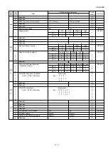
1

DTMF signal transmission level (High)

Binary input

0

2

No. =

16  8   4   2   1

0

3

  1   2   3   4   5

1

4

  0   0   1   0   1

0

5

1

6

0

7

Reserved

0

8

Reserved

0

Reading slice (Binary)

Factory

Light

Dark

Darker in

setting

dark

1

No. 1

0

1

0

1

0

2

No. 2

0

0

1

1

0

Reading slice (Half tone)

Factory

Light

Dark

Darker in

setting

dark

3

No. 3

0

1

0

1

0

4

No. 4

0

0

1

1

0

5

Line density selection

Fine

Standard

0

6

Reserved

0

7

MTF correction in half tone mode

No

Yes

0

8

Reserved

0

1

Number of rings for auto receive

Binary input

0

OPTION

2

No. =

8    4    2    1

1

3

1    2    3    4

0

4

0    1    0    0

0

5

Automatic switching manual to auto receive

Reception after 5 rings

No reception

0

mode

6

Reserved

0

Cl detect frequency

As PTT

11.5Hz

13.0Hz

20.0Hz

7

No.7

0

0

1

1

0

8

No.8

0

1

0

1

0

Distinctive ringing setting

No. 1

No. 2

No. 3

OPTION

(PATTERN 4 and 5 are for CANADA only)

OFF

0

0

0

STANDARD

0

0

1

PATTERN1

0

1

0

PATTERN2

0

1

1

1

PATTERN3

1

0

0

0

2

PATTERN4

1

0

1

0

3

PATTERN5

1

1

0

0

4

Reserved

0

5

Caller ID function

Yes

No

0

OPTION

6

Caller ID detect during CI off

All times

Only first

0

7

Reserved

0

8

Reserved

0

1

Cl off detection timer (0-1550ms setting by

Binary input

0

2

50ms step)

No. =

16  8   4   2   1

1

3

  1   2   3   4   5

1

4

  0   1   1   1   0

1

5

0

6

Reserved

0

7

Reserved

0

8

Reserved

0

SW

NO.

DATA

NO.

ITEM

Switch setting and function

1

0

Remarks

Initial

setting

SW

l

B6

SW

l

C1

SW

l

D2

SW

l

D1

SW

l

D3

Содержание A260 - UX B/W Thermal Transfer

Страница 1: ... description of CIS unit 5 13 CHAPTER 6 CIRCUIT SCHEMATICS AND PARTS LAYOUT 1 Control PWB circuit 6 1 2 TEL LIU PWB circuit 6 9 3 Power supply PWB circuit 6 14 4 Operation panel PWB circuit 6 16 CHAPTER 7 OPERATION FLOWCHART 1 Refer to the service manual of UX P100U 2 Refer to the service manual of UX P100U CHAPTER 8 OTHERS 1 Service tools 8 1 2 Refer to the service manual of UX P100U 3 Refer to t...

Страница 2: ...sti French ATTENTION Il y a danger d explosion s il y a remplacement incorrect de la batterie Remplacer uniquement avec une batterie du même type ou d un type recommandé par le constructeur Mettre au rébut les batteries usagées conformément aux instructions du fabricant Swedish VARNING Explosionsfare vid felaktigt batteribyte Använd samma batterityp eller en ekvivalent typ som rekommenderas av app...

Страница 3: ...er A4 20 lb paper Recording system Thermal transfer recording Halftone grayscale 64 levels Compression scheme MH MR MMR Display 16 digit LCD display Applicable telephone line Public switched telephone network Paper tray capacity Letter Approx 50 sheets 20 lb copier paper at room temperature maximum stack height should not be higher than the line on the tray Legal 5 sheets Recommended paper weight ...

Страница 4: ...ters when storing auto dial numbers 9 Panel release Press this release to open the operation panel 10 STOP key Press this key to cancel operations before they are completed 11 COPY HELP POLL key When a document is in the feeder press this key to make a copy of a document When a document is not in the feeder press this key to print out the Help List a quick reference guide to the operation of your ...

Страница 5: ...and voice calls FAX mode The machine automatically answers all calls and begins fax reception TEL mode Lift the handset when the machine rings Press to begin fax reception TAD mode Select this mode when you go out to receive both voice messages and faxes Note To select TAD mode you must first record an outgoing message START MEMORY TEL LINE Click Fit ends of rolls onto hubs The arrow in the displa...

Страница 6: ...d faxes STORING AUTO DIAL NUMBERS 1 Press FUNCTION once and once 2 Enter a 2 digit Speed Dial number 01 to 40 3 Enter the fax number and press START MEMORY 4 Enter the name by pressing number keys To enter two letters in succession that require the same key press after entering the first letter 5 Press START MEMORY and then STOP 7 Option imaging film specifications UX 5CR 1 Structure This article ...

Страница 7: ...ts below Output voltage settings 3 Settings 1 Dial mode selector DIAL mode Soft Switch No SW B4 DATA No 3 Output Voltage limits 5V 4 25V 5 75V 24V 23 3V 24 7V 2 IC protectors replacement ICPs IC Protectors are installed to protect the motor driver circuit ICPs protect various ICs and electronic circuits from an overcurrent con dition The location of ICPs are shown below 1 24V 2 24V 3 MG 4 MG 5 DG ...

Страница 8: ...s and service soft switch 1 Operating procedure 1 Entering the diagnostic mode Press FUNC 9 8 7 and the following display will appear ROM Ver TB40 After 2 sec DIAG MODE TB40 Then press the START key Select the desired item with the key or the key or select with the rapid key Enter the mode with the START key Diag specifications If the diag mode cannot be set repeat the diag mode operation per form...

Страница 9: ...s used to clear the backup memory and reset to the default settings 3 8 Shading mode The mode is used for the shading compensation For reading set up the special original paper The compensation memorizes the reference data of white and black for reading Moreover the memorized data is not erased even if memory clear mode is executed 3 9 All black print This mode is used to check the state of the pr...

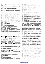
Страница 10: ...tings halfway between SW A1 and SW O6 press the STOP key In this case the setting being done to the SW No on display will be nullified while settings done to the preceding SW No remain in effect The soft switch mode is terminated S F T SW A1 0 0 0 0 0 0 0 0 START DATA No 1 2 3 4 5 6 7 8 When the COPY key is pressed the contents of soft switches are printed 4 How to make soft switch setting To ente...

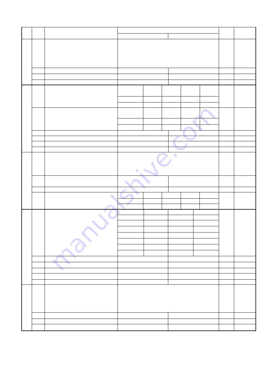
Страница 11: ...unication error 0 sending mode reception 8 CNG transmission No Yes 0 CED tone signal interval 1000ms 750ms 500ms 75ms 1 No 1 1 1 0 0 0 2 No 2 1 0 1 0 0 3 MR coding No Yes 0 4 ECM mode No Yes 0 OPTION 5 ECM MMR mode No Yes 0 6 Reserved 0 7 Reserved 0 8 Reserved 0 1 Signal transmission level Binary input 0 2 No 16 8 4 2 1 1 3 1 2 3 4 5 0 4 0 1 0 0 0 0 5 0 6 Protocol monitor error print Printed at co...

Страница 12: ...eserved 0 8 Reserved 0 1 Reserved 0 2 Reserved 0 3 Reserved 0 4 Reserved 0 5 Reserved 0 Auto dial mode delay timer of before line 0 second 1 5 seconds 3 0 seconds 4 5 seconds 6 connect No 6 0 0 1 1 0 7 No 7 0 1 0 1 0 8 Hold key Enable Disable 1 Auto dial mode delay timer of after line 1 7 seconds 3 0 seconds 3 6 seconds 4 0 seconds 1 connect No 1 0 0 1 1 0 2 No 2 0 1 0 1 0 3 Dial mode Tone Pulse 1...

Страница 13: ...ing manual to auto receive Reception after 5 rings No reception 0 mode 6 Reserved 0 Cl detect frequency As PTT 11 5Hz 13 0Hz 20 0Hz 7 No 7 0 0 1 1 0 8 No 8 0 1 0 1 0 Distinctive ringing setting No 1 No 2 No 3 OPTION PATTERN 4 and 5 are for CANADA only OFF 0 0 0 STANDARD 0 0 1 PATTERN1 0 1 0 PATTERN2 0 1 1 1 PATTERN3 1 0 0 0 2 PATTERN4 1 0 1 0 3 PATTERN5 1 1 0 0 4 Reserved 0 5 Caller ID function Ye...

Страница 14: ...hone Compatible Not compatible 1 5 Remote operation code figure by external Binary input 0 6 TEL 0 9 No 8 4 2 1 1 7 5 6 7 8 0 8 0 1 0 1 1 1 CNG detection in STAND BY mode Yes No 1 OPTION Number of CNG detect AM mode 1pulse 2pulses 3pulses 4pulses 2 No 2 0 0 1 1 0 3 No 3 0 1 0 1 1 Number of CNG detect STAND BY mode 1pulse 2pulses 3pulses 4pulses 4 No 4 0 0 1 1 0 5 No 5 0 1 0 1 1 6 Reserved 0 7 Rese...

Страница 15: ...Busy tone detect intermittent sound detect No Yes 0 Busy tone detection pulse number 2pulses 4pulses 6pulses 10pulses 1 No 1 0 0 1 1 0 2 No 2 0 1 0 1 1 3 Fax switching when A M full Yes No 0 OPTION 4 Busy tone detect continuation sound detect 320Hz 570Hz 320Hz 460Hz 0 frequency 5 Reserved 0 6 Reserved 0 7 AM OGM announce only mode Yes No 0 OPTION 8 Busy tone continuous sound detect time 5s 10s 1 I...

Страница 16: ...7 8 1 8 0 1 1 0 0 1 AGC energy refrence level access code line Binary input 1 2 0 30 dB 2 dB step No 8 4 2 1 0 3 1 2 3 4 1 4 1 0 1 1 1 5 AGC energy refrence level access code Mic Binary input 1 6 0 30 dB 2 dB step No 8 4 2 1 1 7 5 6 7 8 0 8 1 1 0 1 1 1 AGC again adaptation threshold line Binary input 1 2 No 8 4 2 1 1 3 1 2 3 4 1 4 1 1 1 1 1 5 AGC again adaptation threshold Mic Binary input 1 6 No ...

Страница 17: ...munication results printout E T M Send only Always No print Err only OPTION 2 Transaction report No 2 0 0 0 0 1 1 3 No 3 0 0 1 1 0 0 4 No 4 0 1 0 1 0 0 5 OGM ICM output level to speaker Binary input 0 6 0 dB 15 dB 1 dB step No 8 4 2 1 0 7 5 6 7 8 1 8 0 0 1 1 1 1 Reserved 0 2 Reserved 0 3 OGM ICM output level Binary input 0 4 0 dB 32 dB 1 dB step No 32 16 8 4 2 1 0 5 3 4 5 6 7 8 1 6 0 0 1 0 0 1 0 7...

Страница 18: ... Reserved 0 8 Reserved 0 1 Reserved 0 2 Reserved 0 3 Reserved 0 4 Reserved 0 5 Reserved 0 6 Reserved 0 7 Reserved 0 8 Reserved 0 1 Reserved 0 2 Reserved 0 3 Reserved 0 4 Reserved 0 5 Reserved 0 6 Reserved 0 7 Reserved 0 8 Reserved 0 1 Reserved 0 2 Reserved 0 3 Reserved 0 4 Reserved 0 5 Reserved 0 6 Reserved 0 7 Reserved 0 8 Reserved 0 1 Reserved 0 2 Reserved 0 3 Reserved 0 4 Reserved 0 5 Reserved ...

Страница 19: ...erved 0 6 Reserved 0 7 Reserved 0 8 Reserved 0 1 Reserved 0 2 Reserved 0 3 Reserved 0 4 Reserved 0 5 Reserved 0 6 Reserved 0 7 Reserved 0 8 Reserved 0 1 Reserved 0 2 Reserved 0 3 Reserved 0 4 Reserved 0 5 Reserved 0 6 Reserved 0 7 Reserved 0 8 Reserved 0 1 Reserved 0 2 Reserved 0 3 Reserved 0 4 Reserved 0 5 Reserved 0 6 Reserved 0 7 Reserved 0 8 Reserved 0 SW l O3 SW l O4 SW NO DATA NO ITEM Switch...

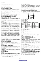
Страница 20: ... to print the content of HEADER PRINT described in the passcode list at the front end of receiver s original when original is sent to the remote machine If this switch is set to NO the HEADER PRINT is not output at the receiving machine SW A2 No 6 Reserved Set to 0 SW A2 No 7 Communication error treatment in RTN sending mode Reception Used to determine communication error treatment when RTN is sen...

Страница 21: ...nd rapid dial calls Use a binary number to program this If set to 0 accidentally 1 will be assumed SW B1 No 5 No 8 Recall times Choice is made as to how many redials there should be SW B2 No 1 Dialing pause sec pause Pauses can be inserted between telephone numbers of direct dial con nection Selection of 4 sec or 2 sec pause is available SW B2 No 2 Dial tone detection before auto dial Used to set ...

Страница 22: ...ter a large number of rings it may not be able to receive faxes successfully If you have diffi culty receiving faxes reduce the number of rings to a maximum of 6 SW D1 No 5 Automatic switching manual to auto receive mode This soft switch is used to select whether the machine should switch to the auto receive mode after 5 rings in the manual receive mode or re main in the same way as SW D1 No 1 No ...

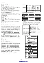
Страница 23: ... 700ms CI interruption 700ms Judged as a CI OFF section The section 1 is not judged as a CI OFF section the CI signal A is counted as one signal The section 2 is judged as a CI OFF section the CI signal B is considered as the second signal 00111 50ms 7 350ms CI interruption 350ms Judged as a CI OFF section The section 1 is judged as a CI OFF section and the CI signal A is counted as two signals Th...

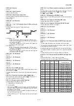
Страница 24: ...C Gain Adaptation Threshold prevents message background noise from corrupting the gain provided that the AGC Gain Adaptation Threshold is greater than the background noise energy In the event that a message has background noise energy greater than the AGC Gain Adaptation Threshold the AGC Gain can be no greater than the AGC Maximum Gain Note that the AGC Gain Adaptation Threshold must always be gr...

Страница 25: ...output level to Line 0dB 32dB 1dB step Used to control OGM and ICM output level to Line SW L1 No 1 No 4 Reserved Set to 0 SW L1 No 5 Cut off mode COPY mode Whether the excessive part is printed on the next recording paper or discarded is selected to copy a document which is longer than the re cording paper SW L1 No 6 A4 Paper enable The use of recording paper of A4 is enabled SW L1 No 7 LEGAL and ...

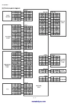
Страница 26: ...OPERATION PANEL TEL LIU PWB UNIT DRIVER MOTOR CONTACT IMAGE SENSOR DOCUMENT SENSOR PIO POWER SUPPLY PWB UNIT AMPLIFIER FAX MODEM DSP CORE SURGE PROTECT FILTER CML TRANSFORMER CI VBT STABILIZER RECTIFIER TRANSFORMER RECTIFIER DIODE TRANS SURGE ABSORBER FILTER LINE CLOCK 32 256MHz LCD FET THERMAL HEAD P IN SENSOR FILM SENSOR RECORDING PAPER FRONT SENSOR SIO S RAM 32kbit IA CX20438 CNPRG AMPLIFIER RE...

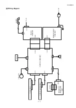
Страница 27: ...NSOR LCD UNIT CNLCD OPERATION PANEL PWB NUIT 14 CNPN A 15 7 CNCSW CNMT CNTH CNCIS CNPN CNSP SPEAKER CNLIUA CNPW 14 6 CONTROL PWB UNIT TEL LIU PWB UNIT POWER SUPPLY PWB UNIT CNLIUA CNPS TEL LINE CNLNJ CNHJ AC CORD TX RX MOTOR 3 HANDSET 4 16 2 Wiring diagram ...

Страница 28: ...N3A KEN2A KEN1A DG 3 3V ORGSNS FRSNS E SEN0 SEN1 SEN2 SEN3 SEN4 SEN5 SEN6 CNPN CNCIS 1 2 3 4 5 6 7 8 9 10 11 12 13 14 1 2 3 4 5 6 7 8 9 10 11 12 13 14 TEL LIU PWB RHS DG 24VL MICMUTE TELIN TELMUTE RXIN TXOUT CML PIN FILM CI HS TELOUT RHS DG 24VL MICMUTE TELIN TELMUTE RXIN TXOUT CML PIN FILM CI HS TELOUT CNLIUA CNLIUA CNMT CNTH 1 2 3 4 5 6 1 2 3 4 5 6 POWER SUPPLY PWB 24V 24V MG MG DG VREG 24V 24V ...

Страница 29: ...r allel to serial form by the modem where the serial data is modulated and sent onto the line Receive operation There are two ways of starting reception manual and automatic Depression of the START key in the off hook mode in the case of manual receive mode or CI signal detection by the LIU in the auto matic receive mode First the SCE214V controls the procedure signals from the modem to be ready t...

Страница 30: ...nded The ROM stores all the program object code 5 Flash Memory Controller The SCE214V includes a flash memory controller that supports NOR NAND and Serial NAND type flash memory The supported size of NOR type memory is up to 1 MB and the supported size of NAND type memory is unlimited 6 Stepper Motor Control Eight outputs are provided to external current drivers four to the scan ner motor and four...

Страница 31: ... frequency as a modulation frequency the output level can be made programmable 18 Watchdog Timer The Programmable Watchdog Timer is intended to guard against firmware lockup on the part of either executive controlled background tasks or interrupt driven tasks and can only be enabled by a sequence of events under control of the Watchdog Control Logic Once the Watch dog Timer has been enabled it can...

Страница 32: ... algorithm includes an optional programmable receive compromise equalizer which is active in both V 23 and Caller ID V 23 Receive only modes Common applications for V 23 include France s Minitel and Japan s Lowest Cost Routing 5 4 4 Features Group 3 facsimile transmission reception ITU T V 17 and V 33 ITU T V 29 V 27 ter T 30 V 21 Channel 2 T 4 ITU T V 17 and V 27 ter short train HDLC framing at a...

Страница 33: ...IA The LSB of each 16 bit address contents is used to control the PIA The MSB of each 16 bit address contents is used to control the SIA The following table the PIA SIA control register RAM access code 5 5 Fig 3 PIA SIA Signal Flow Control Register SBRAMx BRx Crx IOx AREXx ADDx PIA Reg SIA Reg For changes made to IACR1 to be effective the host must write to IAADD with a value of 0002h For changes ...

Страница 34: ...OUT O Osc1 31 WRPROTn O 1XC 32 TEST 1 I Hd 33 TEST 0 I Hd 34 BATRSTn I H 35 INTPWRDWNEn I H 36 PWRDWNn I O H 13Xs 37 N C 38 ADGA VADG PADC Analog GND 39 VREFn CLREF I VR PADC 40 VIN I VA PADC 41 ADGA VADG PADC Analog GND 42 ADVA VADV PADC Analog Power 43 ADXG VXG PADC 44 VREFp I VR PADC 45 VSS VSS Digital GND 46 IVREFn O VR PADC 47 IVREFp O VR PADC 48 VDD Digital Power 49 THADI I Analog TADC 50 VS...

Страница 35: ...Digital GND 94 FCSn 1 VIDCTL 0 GPO 23 O 13Xs 95 IARESET O 13Xs DSP to EXTIA POR 96 IACLK O 13Xs DSP to EXTIA MCLK 97 VDD Digital Power 98 IA1CLK I H DSP from EXTIA ICLK 99 SR3IN DSPIRQn I H DSP from primary EXTIA SOUT EXT Modem IRQn 100 SR4OUT O 13Xs DSP to primary EXTIA SIN 101 SR1IO O 13Xs DSP to EXTIA CTRL1 102 SA1CLK I H DSP from EXTIA FSYNC 103 GPIO 7 SSRXD2 SASRXD2 I O Hu 13Xs 104 GPIO 6 SST...

Страница 36: ...s 146 D 5 I O Tu 13Xs CPU Data Bus 147 D 6 I O Tu 13Xs CPU Data Bus 148 D 7 I O Tu 13Xs CPU Data Bus 149 GPIO 20 ALTTONE I O Hu 13Xs 150 GPIO 26 I O Hu 13Xs 151 GPIO 27 I O Hu 13Xs 152 GPIO 28 I O Hu 13Xs 153 GPO 26 O 13Xs 154 GPO 27 O 13Xs 155 GPO 28 O 13Xs 156 GPO 29 O 13Xs 157 GPO 30 SR3OUT O 13Xs 158 GPIO 29 I O Hu 13Xs 159 GPIO 31 I O Hu 13Xs 160 GPIO 32 I O Hu 13Xs 161 VDD Digital power 162 ...

Страница 37: ...CRYSTAL SCANNER CONTROLS SENSORS START CLK2 CLK1 CLK1N VIDCTL 1 0 XIN XOUT INTERNAL IA LINE INTERFACE DRAM SCANNER VIDEO PREPROCESSING SERIAL SYNC PORTS SSIF VIN VREFP VREFN SSCLK 2 1 SSTXD 2 1 SSRXD 2 1 SSSTAT 2 1 SYNC ASYNC SERIAL PORT SASIF SASCLK SASTXD SASRXD GPIO GENERAL PURPOSE I O DEBUGN VDD VDRAM VBAT VSS FLASH MEMORY OPTION WRPROTN FRDN FRWN FCLE FCSN 2 0 D 7 0 RDN A 23 0 WRN ROMCSN CS 5...

Страница 38: ... the combination of the attenuator value of the LINE DRIVER in the modem and the ringer sending level sent from the modem Speaker volume It is controlled by the attenuator value of the IC5 and IC3 VOL A B C 4 Ringer circuit section The ringer sound is formed in the tone of modem when CI signal is detected The amplifier circuit drives the speaker of the main body 5 10 DAC LPF DAC H L CI DETECTOR SP...

Страница 39: ...1 0 Level4 0 1 0 Level5 1 0 0 Ringer volume setting Low 1 1 1 Middle 0 0 1 High 0 0 0 DTMF speaker volume Level1 1 0 1 setting Level2 1 0 1 Level3 1 0 1 Level4 1 0 1 Level5 1 0 1 OGM playback speaker Level1 0 0 1 volume setting Level2 1 1 0 Level3 0 1 0 Level4 1 0 0 Level5 0 0 0 ICM record speaker Level1 0 0 1 volume setting Level2 1 1 0 Level3 0 1 0 Level4 1 0 0 Level5 0 0 0 Signal Name Descripti...

Страница 40: ...AKER LINE 24VL DG CONTROL PWB TEL LIU PWB RX TX TEL MUTE H MUTE PC2A Q101 IC7 IC101 B Q102 IC101 C Q105 Q104 IC101 D IC101 A IC5 0 1 0 0 1 0 1 1 RTLOOP ADC SIN MIC LINE SELECT MODEM BLOCK 20438 I A SP OUT ENABLE MIC ENABLE LINE IN ENABLE LINE OUT ENABLE 0 20 25 30dB LINESEL 1 1 0 0 1 0 0 4dB SOUT SPKRP MICP LINEIN LINE OUT MUTE 0 6 12dB IC3 SCE214V FAX CONTROLLER DTMFMUTE BZOUT1 RCVOL SP MUTE TEL ...

Страница 41: ...Noise filter circuit The input noise filter section is composed of L1 and C1 which reduces normal mode noise from the AC line and common mode noise to the AC line 2 2 Rectifying smoothing circuit The AC input voltage is rectified by diode D1 2 3 4 and smoothed by capacitor C2 to supply DC voltage to the switching circuit section 2 3 Switching circuit This circuit includes MOS FET Q1 and the gate d...

Страница 42: ... 127 A11 126 A10 125 A9 124 A8 123 A7 122 A6 121 A5 120 A4 118 A0 114 A3 117 A2 116 A1 115 RD 6 WR 5 ROMCS 3 SYNC 4 REGDMA GPO18 CLKDIV0 175 WAIT GPO19 CLKDIV1 176 RAS 25 CAS 26 DWR 27 WRPROT 31 BATRST 34 VBAT 28 PWRDWN 36 INTPWRDOWNE 35 XOUT 30 XIN 29 VREFp 44 VREFn CLREF 39 VIN 40 THADI 49 ALTTONE BZ 149 OPI0 19 OPI1 20 OPI2 21 OPI3 22 SM0 171 SM1 172 SM2 173 SM3 174 OPO0 12 OPO1 13 OPO2 14 OPO3...

Страница 43: ... 12 A13 4 A14 5 A15 11 A16 10 A17 6 CE 30 OE 32 WE 7 D0 21 D1 22 D2 23 D3 25 D4 26 D5 27 D6 28 D7 29 VDD 8 GND 24 N C A18 9 C218 0 1u 50V R125 10k R112 10k C100 0 1u 50V IC2 DRAM MSM51V4800E OKI IS41LV85125 ISSI VCC 1 WE 7 RAS 8 A9 9 VCC 14 GND 15 OE 22 CAS 23 GND 28 DQ0 2 DQ1 3 DQ2 4 DQ3 5 DQ4 24 DQ5 25 DQ6 26 DQ7 27 A0 10 A1 11 A2 12 A3 13 A4 16 A5 17 A6 18 A7 19 A8 20 NC 6 NC 21 R115 N M C126 0...

Страница 44: ... 8 7 6 2 3 4 IC3 SCE214V 2 2 MODEM BLOCK GPIO15 CS5 53 GPIO16 52 AVDD IIA 85 GPIO37 55 GPO28 155 GPIO31 159 GPO27 154 GPO25 68 GPIO34 162 GPO30 157 GPIO32 160 GPIO13 54 GPIO17 51 SPKR_OUTP IIA 88 GPO1 168 MIC_INM IIA 81 MIC_INP IIA 80 GPO29 156 MCDE0 91 GPO0 167 LINE_INP IIA 79 N C 37 SASRXD 110 GPIO3 109 GPIO19 66 GPIO11 65 GPIO36 164 GPIO35 163 VTHON 56 MIC_BIAS IIA 82 TESTC 73 FCS 94 GPIO29 158...

Страница 45: ...G MG MG 3 3A 1 1G DG 3 3A 3 3A 3 2A 3 3A FILM ORGSNS DG DG DG 3 3V DG DG DG DG DG DG MG FG 3 3V D100 HRW0202 A1 A2 K C207 1000p 50V C105 1000p 50V D101 1SS355 A K L102 0 R179 270 BAT1 CR2032 R103 270 C211 470p 50V R166 20k R127 51K R102 270 R100 5 6K R111 N M 2 5 IC10 4 3 1 R168 270 C106 1000p 50V C158 C157 C171 100p 50V R170 N M REG1 S 814A33AUA Vin 3 Vout 1 VSS 2 R202 C9 47u 25V R147 R181 C193 0...

Страница 46: ...5H D YNA ROHM 0Ω N M N M 0 01u 50V 300Ω 2W 1000p 50V R1 R192 C124 CIS Maker 1 1E 1 1E 1 1E 3 4A 3 2A 1 1F DG DG DG DG DG DG DG DG DG THG THG R1 N M R172 22K C154 N M C117 0 1u 50V R174 1K R149 10k R192 0 C114 0 1u 50V Q100 2SA1530A B C E R152 20K R150 470K R171 120K R129 1K C1 220u 6 3V IC6 ULN2001A E 8 1B 1 2B 2 3B 3 4B 4 5B 5 6B 6 7B 7 7C 10 6C 11 5C 12 4C 13 3C 14 2C 15 1C 16 COM 9 Q102 RT1N141...

Страница 47: ...X7 X B VDD GND VEE E IC5 IC4 16 7 11 10 9 6 3 13 14 15 12 1 5 2 4 8 R121 150K D102 1SS355 R137 20K Q104 RT1N141C B C E C212 0 1u 50V Q112 B C E ZD101 N M C208 1u 10V K C189 1u 10V R164 1M R180 39K R184 R194 C2 47u 25V 1 2 C187 0 1u 16V K R143 39K R144 24K C182 1u 10V K C181 0 R140 470K R142 200K R138 N M R122 100K C186 0 C156 0 1u 50V R146 91K C125 1u 10V C150 1u 10V R136 3K R124 220K R145 6 2K R1...

Страница 48: ...UX A260U Control PWB parts layout Top side 6 7 manuals4you com manuals4you com ...

Страница 49: ...UX A260U Control PWB parts layout Bottom side 6 8 ...

Страница 50: ...1 RA 391P V6 2 ZD4 J P R11 PC3A PC814X R111 100 ZD10 HZ2A1 12 5mm C13 L3 ZD9 HZ2A1 12 5mm C137 2125 1608 N M L7 C7 JP R7 91 1 4W REC1 R8 30 1 4W R12 22k 1 2W JP2 N M N M N M JP7 JP C11 N M L6 R10 D2 1N4148 ZD5 HZ27 L2 JP6 N M N M CML 1 3 A5X 24E 908 3 5 4 C5 22u 50 Q2 G D S R132 0 2125 1608 L5 T1 i2164 R13 JP 1W Q1 B C E C 122 N M N M R3 PC4A PC817X4 2 1 R133 2125 1608 22k JP3 JP ZD6 HZ2C1 C109 10...

Страница 51: ...0 N M R120 13k R125 1 5k C136 R116 3 6k R129 C108 1000p C133 R14 150 1 4W R113 620 E Q104 RT1N436 B C R127 C135 N M C125 0 JP8 N M R130 8 2k JP4 N M C126 470p C112 820p C113 N M R134 N M N M C127 N M ZD1 HZ9C3 C116 1000p C119 0 1u C12 4 7u 50V Q103 RT1P141C B C E C131 N M R119 8 2k IC101C NJM2902 9 10 O 8 C104 N M R114 0 R107 22k C134 0 1u 16V R115 3 3k C128 N M D100 1N4148 L4 LSHSR02C 001 C130 22...

Страница 52: ...HS DPMUTE CML RHS 24VL FILM Ci DG PIN N M Q100 B C E C102 N M C106 1000p C121 Vref A PC3B PC814X 4 3 D3 1N4148 R112 0 PC2B N M 4 3 SW1 HOOK SW 3 1 2 PC4B PC817X4 4 3 C3 N M PH1 SG206S R101 2125 1608 C103 0 1u 2125 1608 C115 0 1u 2125 1608 C1 22u 50V PC1B 2 1 IC101 HA17324A 4 11 R1 1 2k 1W D1 14148 C101 0 1u 2125 1608 C2 100u 50V Q102 RT1N436 B C E R124 TP1 JP PH2 SG206S REG 1 N JM 78L 05A Vout 1 G...

Страница 53: ...UX A260U TEL LIU PWB parts layout Top side 6 12 ...

Страница 54: ...UX A260U TEL LIU PWB parts layout Bottom side 6 13 manuals4you com manuals4you com ...

Страница 55: ...5V GND GND GND 1 2 6 3 4 5 6 8K N M R27 6 8K R29 6 8K ZD4 HZ30CPTK ZD9 RD9 1ESAB2 T1 ZD8 RD10ESAB T1 R13 4 7K R14 1K R16 10K C12 0 1 VR1 2 2K R17 3 3K ZD5 RD6 2SAB2 T1 R15 330K Q4 2SC1740S R18 3 3K PC1 PS2501 1L C10 330 16 D8 ERA81 004V3 D7 S3L20U FB3 BP53RB052025050 D9 ERA22 06V3 R3 470K C26 C3 470P Q1 2SK3306 ZD1 27HSB 26 C27 0 01 0 01 L1 33mH 0 5A C1 0 22 V1 S07K150GA F1 R10 R9 47 Q3 2SC1741AS ...

Страница 56: ...UX A260U Power supply PWB parts layout Top side 6 15 Power supply PWB parts layout Bottom side manuals4you com manuals4you com ...

Страница 57: ...13 CNLCD 12 CNLCD 2 CNLCD 14 CNLCD 11 CNLCD 5 CNLCD 3 E KEN4A CNPN RS E CNLCD 6 3 3V 4 1 R W 9 VO N C 8 2 7 5 3 LD2 LD1 10 LD0 LD3 11 12 13 14 CNPN 1 CNPN 4 CNPN 2 CNPN 3 SEN2 SEN3 SEN0 SEN4 KEN3A KEN1A KEN2A SEN5 3 3V ORGSNS FRSNS SEN1 DG N C N C N C SEN6 DG 6 2 12 7 14 13 5 10 11 1 8 9 3 4 15 16 D 5 1SS133 A K 5 8 START R4 10k UP R1 10k DOWN R5 10k 4 A R6 N M 10k C 1 0 022u 50V 0 7 KEY 1 KEY 3 R...

Страница 58: ...UX A260U 6 17 Operation panel PWB parts layout Top side Operation panel PWB parts layout Bottom side Note Since the parts of PWB cannot be supplied change it as a unit manuals4you com manuals4you com ...

Страница 59: ...UX A260U 6 18 CHAPTER 7 OPERATION FLOWCHART 1 Protocol Refer to the service manual of UX P100U 2 Power on sequence Refer to the service manual of UX P100U ...

Страница 60: ...TY PRICE RANK 1 CPWBF3201SCS1 Extension board unit TEL LIU PWB 1 BA 2 PSHEZ3579SCZZ Shading wave memory standard paper 1 AD Extension board unit 1 QCNWG471BSCZZ SPEAKER RELAY CABLE 1 2 QCNWG206BSCZZ PANEL RELAY CABLE 1 AT 3 QCNWG202BSCZZ CIS RELAY CABLE 1 AN 4 QCNWG205BSCZZ HEAD RELAY CABLE 1 AS 5 QCNWG204BSCZZ CAM SWITCH RELAY CABLE 1 AG 6 QCNWG242BSCZZ MOTOR RELAY CABLE 1 AM 7 QCNWG201BSCZZ SENS...

Страница 61: ...replaced with the parts specific to the product specification 1 Cabinet etc 2 Top cover Sub frame 3 Upper cabinet Document guide upper 4 Drive unit 5 Packing material Accessories 6 Control PWB unit 7 TEL LIU PWB unit 8 Power supply PWB unit 9 Operation panel PWB unit Index UX A260 MODEL MODEL SELECTION CODE DESTINATION UX A260 U U S A ...

Страница 62: ...DOCUMENT GUIDE UPPER TOP COVER SUB FRAME DRIVE UNIT 27 22 30 31 28 25 26 26 29 4 57 35 54 46 50 52 51 53 3 5 36 37 58 48 47 6 17 49 41 42 45 7 61 44 43 59 29 25 24 33 34 32 63 23 64 65 67 8 68 69 16 B2 B1 B1 B1 B1 B1 B1 B2 B3 B2 W1 B4 W2 B1 B5 manuals4you com manuals4you com ...

Страница 63: ...340XHZA AD C Head spring C 41 PCOVP2130XHZZ AE C Head cover 42 PGIDM2615XHZZ AD C Head guide left 43 PGIDM2616XHZZ AD C Head guide right 44 QCNWN486AXHZZ AM C Head cable 45 RHEDZ2065XHZZ BP B Thermal head 46 GCOVA2447XHVA AL N D Front cover 47 GLEGG2078XHZZ AD C Rubber leg 48 LPLTM3178XHZZ AF C Bottom plate 49 LPLTP3177XHZZ AD C Stopper plate 50 MLEVP2357XHZZ AD C Film sensor lever 51 MLEVP2356XHZ...

Страница 64: ...t 17 PGIDM2621XHSA AF C Release lever 18 LHLDZ2224XHZZ AL C RP feed plate holder 19 LPLTG3181XHZZ AD C RP separate rubber 20 LPLTP3179XHZZ AD C RP separate base 21 LPLTP3180XHZZ AH C RP separate plate 22 LPLTP3182XHZZ AH C RP feed plate 23 MSPRC3299XHZZ AB C RP separate spring 24 MSPRC3300XHZZ AB C RP feed spring 25 LBSHP2148XHZA AE N C Platen bearing left 26 LBSHP2149XHZA AE N C Platen bearing ri...

Страница 65: ...HZZ AE C ORGSNS sensor 9 QCNWN425BXHZZ AR N C Panel cable 10 RUNTZ2127XH01 BC N E LCD unit 11 LPLTG2911XHZZ AE C Separate rubber 12 LPLTP3175XHZZ AD C Separate plate 13 LPLTP3176XHZZ AD C Feed plate 14 MSPRD3293XHZZ AB C Separate spring 15 MSPRT3294XHZZ AB C Feed spring 16 PGIDM2614XHSA AL C Document guide upper 17 PSHEP3660XHZZ AE C Separate rubber sheet 18 JBTN 2360XHSC AH N C Speed key 19 JBTN ...

Страница 66: ...GERH2380XHZZ AC C Reduction gear 17 36Z 11 NGERH2409XHZZ AB C Idler gear 23Z 12 NGERH2571XHZZ AD C Slip gear 13 NGERH2572XHZZ AD C Reduction gear 25 63Z 14 NGERH2573XHZZ AD C Reduction gear 20 40Z 15 NGERH2574XHZZ AD C Reduction gear 15 30Z 16 NGERH2575XHZZ AD C Idler gear 40Z 17 NGERH2576XHZZ AD C Idler gear 21Z 18 NGERH2577XHZZ AD C Idler gear 20Z 19 NGERH2582XHZZ AC C Idler gear 15Z 20 QCNWN483...

Страница 67: ...11 TINSE4356XHTZ AY N D Operation manual 12 TCADZ3599XHZZ AP N D Pop label 14 SPAKA465CXHZZ AF D Packing add left 15 SPAKA466CXHZZ AF D Packing add right 16 SPAKA467CXHZZ AD D Packing add accessories 17 CPAKC222FXH01 AT N D Packing case with label 18 SPAKP329DXHZZ AF D Vinyl cover 20 CPLTP3183XHRF AV N C Paper tray ass y 21 CGERH2566XH01 AG C Imaging film gear ass y 6 5 Packing material Accessorie...

Страница 68: ...C Capacitor 10WV 1µF C140 39 VCKYCY1HF104Z AA C Capacitor 50WV 0 1µF C141 40 VCKYCY1AF105Z AC C Capacitor 10WV 1µF C142 41 VCKYCY1AF105Z AC C Capacitor 10WV 1µF C143 42 VCKYCY1AF105Z AC C Capacitor 10WV 1µF C144 43 VCKYCY1AF105Z AC C Capacitor 10WV 1µF C145 44 VCCCCY1HH200J AA C Capacitor 50WV 20PF C146 45 VCKYCY1AF105Z AC C Capacitor 10WV 1µF C147 46 VCKYCY1AF105Z AC C Capacitor 10WV 1µF C148 47 ...

Страница 69: ...N141C Q113 119 VRS CY1JB562J AA C Resistor 1 16W 5 6KΩ 5 R100 120 VRS CY1JB103J AA C Resistor 1 16W 10KΩ 5 R101 121 VRS CY1JB271J AA C Resistor 1 16W 270Ω 5 R102 122 VRS CY1JB271J AA C Resistor 1 16W 270Ω 5 R103 123 VRS CY1JB000J AA C Resistor 1 16W 0Ω 5 R104 124 VRS CY1JB471J AA C Resistor 1 16W 470Ω 5 R105 125 VRS CY1JB471J AA C Resistor 1 16W 470Ω 5 R106 126 VRS CY1JB103J AA C Resistor 1 16W 10...

Страница 70: ...k resistor 470Ωx4 RA2 195 RR TZ3018SCZZ AC C Block resistor 470Ωx4 RA3 196 RR TZ3017SCZZ AC C Block resistor 270Ωx4 RA4 197 RH IX2357XHZZ AH B IC S 814A33AUA REG1 198 RCRSP2176SCZZ AG B Crystal 32 256MHz X1 199 RCRSB0297AFZZ AD B Crystal 32 768kHz X2 200 VHE1N4748A 1 AC B Diode 1N4748A ZD1 201 VHE02CZ180Y 1 AC B Zener diode 02CZ180Y ZD100 Unit 901 DCEKC481SXHZZ BY N E Control PWB unit Within ROM 7...

Страница 71: ...CY1JB822J AA C Resistor 1 16W 8 2KΩ 5 R119 72 VRS CY1JB133J AA C Resistor 1 16W 13KΩ 5 R120 73 VRS CY1JB822J AA C Resistor 1 16W 8 2KΩ 5 R121 74 VRS CY1JB224J AA C Resistor 1 16W 220KΩ 5 R122 75 VRS CY1JB102J AA C Resistor 1 16W 1KΩ 5 R123 76 VRS CY1JB152J AA C Resistor 1 16W 1 5KΩ 5 R125 77 VRS CY1JB332J AA C Resistor 1 16W 3 3KΩ 5 R126 78 VRS CY1JB822J AA C Resistor 1 16W 8 2KΩ 5 R130 79 VRS CY1...

Страница 72: ...ilm resistor 1W 0 15Ω 5 R10 47 0CBUEXDAW334 AC N C Resistor 1 4W 330KΩ 5 R11 48 0CBUEXDAW334 AC N C Resistor 1 4W 330KΩ 5 R12 49 0CBUEEB472CT AC C Resistor 1 4W 4 7KΩ 5 R13 50 0CBUEXCAP102 AC C Resistor 1 16W 1KΩ 5 R14 51 0CBUEXBAF334 AC N C Resistor 1 16W 330KΩ 5 R15 52 0CBUEXBAF103 AC N C Resistor 1 16W 10KΩ 5 R16 53 0CBUEXBAF332 AC N C Resistor 1 16W 3 3KΩ 5 R17 54 0CBUEEB332CT AC N C Resistor ...

Страница 73: ...NGERH2577XHZZ 4 18 AD C NGERH2579XHZZ 2 27 AD C NGERH2580XHZZ 2 11 AC C NGERH2581XHZZ 2 12 AC C NGERH2582XHZZ 4 19 AC C NGERP2318XHZZ 2 3 AD C NROLP2332XHZZ 1 29 AD C NROLR2482XHZZ 1 30 AR C NROLR2483XHZZ 2 13 AL C NROLR2485XHZZ 2 28 AQ C NROLR2504XHZZ 2 14 AL N C NSFTP2357XHZZ 2 15 AG C NSFTP2374XHZZ 2 16 AG N C P PBRS 2055XHZZ 1 63 AN C PCOVP2130XHZZ 1 41 AE C PCOVP2131XHVA 1 57 AG N C PCOVP2132...

Страница 74: ... 6 132 AA C 6 141 AA C 6 142 AA C 6 144 AA C 6 147 AA C 6 162 AA C 6 176 AA C 7 70 AA C 7 75 AA C 7 79 AA C VRS CY1JB103J 6 120 AA C 6 126 AA C 6 128 AA C 6 138 AA C 6 158 AA C 6 160 AA C 6 165 AA C 6 189 AA C 6 190 AA C 6 191 AA C VRS CY1JB104J 6 136 AA C 6 192 AA C VRS CY1JB105J 6 145 AA C 6 168 AA C VRS CY1JB106J 6 166 AA C VRS CY1JB124J 6 173 AA C VRS CY1JB133J 7 72 AA C VRS CY1JB150J 6 109 AA...

Страница 75: ...C C 0CBUEEB682CT 8 55 AC C 8 56 AC C 8 57 AC C 0CBUEFDR15DB 8 46 AE C 0CBUEFE104DS 8 58 AE N C 0CBUEXBAF000 8 6 AC N C 0CBUEXBAF103 8 52 AC N C 0CBUEXBAF181 8 43 AC N C 0CBUEXBAF183 8 42 AC N C 0CBUEXBAF332 8 53 AC N C 0CBUEXBAF334 8 51 AC N C 0CBUEXBAF470 8 45 AC N C 0CBUEXBAF473 8 44 AC N C 0CBUEXCAP102 8 50 AC C 0CBUEXCAP272 8 41 AC C 0CBUEXDAW334 8 37 AC N C 8 47 AC N C 8 48 AC N C 0CBUEXDAW47...

Страница 76: ... in U S A A0308 1100DS IS T No part of this publication may be reproduced stored in a retrieval system or transmitted in any form or by any means electronic mechanical photocopying recording or otherwise without prior written permission of the publisher COPYRIGHT 2003 BY SHARP CORPORATION ALL RIGHTS RESERVED manuals4you com manuals4you com ...

Отзывы: