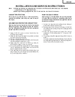


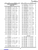

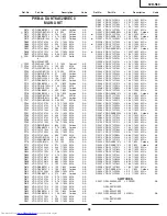


14
32R-S60
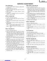
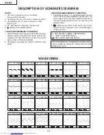
DESCRIPTION OF SCHEMATIC DIAGRAM
NOTES:
1. The unit of resistance "ohm" is omitted.
(K=k
Ω
=1000
Ω
, M=M
Ω
)
2. All resistors are 1/8 watt, unless otherwise noted.
3. All capacitors are
µ
F, unless otherwise noted.
(P=pF=
µµ
F)
4. (G) indicates
±
2% tolerance may be used.
5.
indicates line isolated ground.
VOLTAGE MEASUREMENT CONDITIONS:
1. All DC voltages are measured with DVM connected
between points indicated and chassis ground, line
voltage set at 120V AC and all controls set for normal
picture unless otherwise indicated.
2. All voltages measured with 1000
µ
V B & W or Color
signal.
WAVEFORM MEASUREMENT CONDITIONS:
1. Photographs taken on a standard gated color bar
signal, the tint setting adjusted for proper color. The
wave shapes at the red, green and blue cathodes of
the picture tube depend on the tint, color level and
picture control.
2.
indicates waveform check points (See chart,
waveforms are measured from point indicated to
chassis ground.)
WAVEFORMS
1
1.2 Vp-p
2
2.3 Vp-p
3
1.0 Vp-p
4
0.5 Vp-p
5
5
Vp-p
6
5
Vp-p
7
1.1 Vp-p
8
1.5 Vp-p
9
30
Vp-p
0
53
Vp-p
q
5.4 Vp-p
w
0.8 Vp-p
e
190 Vp-p
r
15
Vp-p
t
1050 Vp-p
y
900 Vp-p
u
220 Vp-p
i
27
Vp-p
o
3.0 Vp-p
p
3.0 Vp-p
a
3.0 Vp-p
s
140 Vp-p
d
130 Vp-p
f
130 Vp-p
å
AND SHADED (
) COMPONENTS
= SAFETY RELATED PARTS.
ç
MARK= X-RAY RELATED PARTS.
This circuit diagram is a standard one, printed circuits
may be subject to change for product improvement
without prior notice.
Содержание 32R-S60
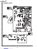
Страница 12: ...12 6 5 4 3 2 1 A B C D E F G H 32R S60 CHASSIS LAYOUT ...
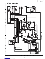
Страница 13: ...13 6 5 4 3 2 1 A B C D E F G H 32R S60 BLOCK DIAGRAM ...
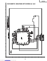
Страница 15: ...15 6 5 4 3 2 1 A B C D E F G H 32R S60 SCHEMATIC DIAGRAM MTS MODULE Unit ...
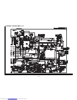
Страница 16: ...16 17 1 2 3 4 5 6 7 8 9 10 11 12 13 14 15 16 17 18 19 20 A B C D E F G H I J SCHEMATIC DIAGRAM MAIN 1 Unit ...
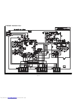
Страница 17: ...18 19 1 2 3 4 5 6 7 8 9 10 11 12 13 14 15 16 17 18 19 20 A B C D E F G H I J SCHEMATIC DIAGRAM MAIN 2 Unit ...
Страница 18: ...20 21 1 2 3 4 5 6 7 8 9 10 11 12 13 14 15 16 17 18 19 20 A B C D E F G H I J SCHEMATIC DIAGRAM AV Unit ...
Страница 19: ...22 6 5 4 3 2 1 A B C D E F G H 32R S60 SCHEMATIC DIAGRAM CRT Unit ...
Страница 21: ...24 6 5 4 3 2 1 A B C D E F G H 32R S60 PWB A MAIN Unit Wiring Side ...
Страница 22: ...25 6 5 4 3 2 1 A B C D E F G H 32R S60 PWB A MAIN Unit Chip Parts Side ...
Страница 23: ...26 6 5 4 3 2 1 A B C D E F G H 32R S60 PWB C AV Unit Chip Parts Side PWB C AV Unit Wiring Side ...