27U-S650
10
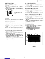
Sub-Tint Adjustment
1. Receive the half color bar signal.
•
RF INPUT
2. Get into Y-Mute by R/C, or by setting the "V18" bus
data to "01".
3. Vary the "V02" bus data until the waveform becomes
as stated below.
•
AV INPUT
5. Input data of "V41" to minus 5 step from "V02" data.
Sub-Color Adjustment
1. Receive a good local channel.
2. Make sure the customer color control is set to center
position .
3. Enter the service mode and select service adjustment
"V03".
4. Adjust "V03" data value to obtain normal color level.
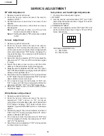
Figure B.
LEVEL
B-AMP Base waveform in step
(TP47B)
Vertical-Size and Linearity Adjustments
1. Receive a good local channel.
2. Enter the service mode and select the service
adjustment "D03" for V-size.
3. Adjust the "D03" bus data to get the proper V-size.
4. For V-linearity adjustment, select data bus "D05" and
adjust to get the proper vertical linearity.
Note: Aging for 10 min before adjustment. After the
adjustment of V-phase and V-size, re-
adjustment for this V-line.
Vertical Phase Adjustment
1. Enter the service mode and select the service
adjustment "D01".
2. Adjust "D01" data value so that picture is centered.
Horizontal Position Adjustment
1. Receive a good local channel.
2. Enter the service mode and select the service
adjustment "D02".
3. Adjust "D02" data value so that picture is centered.
Caption Position Adjustment (Horizontal)
1. Receive a good local channel.
2. Enter the service mode and select the service
adjustment "EX2".
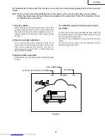
3. A black text box appears on the screen. (see
Figure
B. below)
4. Adjust "EX2" data value so that text box is positioned
in the center of the screen.
Other Adjustments
1. Enter the service mode.
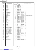
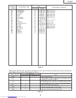
2. Adjust the following data values as listed below.
SERVICE ADJUST DATA(Hex)
POSITION ITEM
OP1 OPTION1 F5
OP2 OPTION2 10
OP3 OPTION3 0E
Содержание 27U-S650
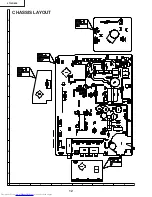
Страница 12: ...12 6 5 4 3 2 1 A B C D E F G H 27U S650 CHASSIS LAYOUT ...
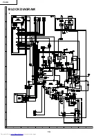
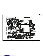
Страница 13: ...13 6 5 4 3 2 1 A B C D E F G H 27U S650 BLOCK DIAGRAM ...
Страница 15: ...16 27U S650 15 12 11 10 9 8 7 6 5 4 3 2 1 A B C D E F G H ...
Страница 16: ...16 18 27U S650 17 12 11 10 9 8 7 6 5 4 3 2 1 A B C D E F G H ...
Страница 17: ...20 27U S650 19 12 11 10 9 8 7 6 5 4 3 2 1 A B C D E F G H ...
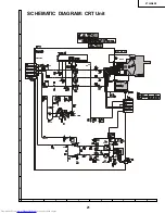
Страница 18: ...21 27U S650 6 5 4 3 2 1 A B C D E F G H SCHEMATIC DIAGRAM CRT Unit ...
Страница 19: ...22 6 5 4 3 2 1 A B C D E F G H 27U S650 DIAGRAM MTS MODULE Unit ...
Страница 20: ...27U S650 6 5 4 3 2 1 A B C D E F G H 23 PRINTED WIRING BOARD ASSEMBLIES PWB A MAIN Unit Wiring Side ...
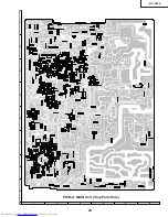
Страница 21: ...27U S650 6 5 4 3 2 1 A B C D E F G H 24 PWB A MAIN Unit Chip Parts Side ...
Страница 22: ...25 6 5 4 3 2 1 A B C D E F G H 27U S650 PWB C AV Unit Wiring Side PWB C AV Unit Chip parts Side ...
Страница 24: ...27 6 5 4 3 2 1 A B C D E F G H 27U S650 PWB B CRT Unit Wiring Side ...


