7
7-1
7-2
14EM4RU
21EM4RU
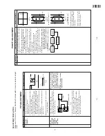
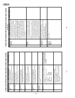
PIF ADJUSTMENT
No.
Adjusting point
Adjusting procedure/conditions
W
aveform and others
T
uner IFT
( PRESET )
1
1
.
Get the tuner ready to receive the CH. E - 9
signal,but with no signal input.
Adjust the PLL data.
2
.
Connect the sweep generator's output cable to
the tuner antenna. ( RF SWEEP )
3.
Adjust the sweep generator's to 80dBuV
.
4.
Connect the response lead ( use LOW IMPED-
ANCE probe with wave detector ; see Fig.1 ) to
the tuner's IF output terminal. (
This terminal
must have the probe alone connected ).
5
.
Set the RF
AGC to 0 - 6 V with no saturation with
the waveform.
6
.
Adjust the tuner IF coil to obtain the waveform as
shown in Fig. 2.
Note:
B
e
sure to keep the tuner cover in position
during this adjustment.
RF-AGC
T
AKE OVER
POINT AD-
JUSTMENT
(I
2
C BUS
CONTROL)
1.
Receive "P
AL
COLOUR BAR" signal.
»
Signal Strength: 57
±
1 dB
µ
V (75 ohm open)
2.
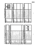
Connect the oscilloscope to
TP201(T
uner
’s
AGC
T
erminal) as shown in Fig. 3.
3
.
Call "AGC" mode in service mode.
Adjust the
"AGC" bus data to obtain the
T
uner output pin
drop 0.1V below maximum voltage.
4.
Change the antenna input signal to 63~67dB
µ
V,
and make sure there is no noise.
5
.
T
urn up the input signal to 90~95 dB
µ
V to be sure
that there is no cross modulation beat.
Note: For the 50 ohm signal
strength gauge, when not
using 50/75 impedance
adapter
, signal strength is
52
±
1dB
µ
V(75 ohm open), in-
stead of 57
±
1dB
µ
V (75 ohm
open).
Precaution: The loss of using
impedance adapter
2
Fig. 3
Fig.1
Fig.2
»
Bias bo
x:
About 4.5
V
Oscilloscope
0.1V
TV Set
Bias box
TP210
+
+
–
–
E-9 CH
P
C
10k
100k
1n60
75ohm
IF OUT
-1.5+/-0.8dB
1000p
Oscilloscope
ADJUSTMENT PRECAUTION:
Make sure
TV Set is in "Normal Condition" before switch to service mode for adjust-
ment.
PURITY
ADJUSTMENT
No.
Adjusting point
Adjusting procedure/conditions
W
aveform and others
PURITY
ADJ.
1
.
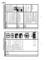
Receive the GREEN-ONL
Y
signal.
Adjust the
beam current to about 500
µ
A (14") and 700
µ
A
(21").
2
.
Degauss the CR
T
enough with the degausing coil.
Note:
Follow the Job Instruction Sheet to ad-
just the magnetic field.
3.
Maintain the purity magnet at the zero magnetic
field and keep the static convergence roughly
adjusted.
4
.
Observe the points a, b as shown in Fig. 4-1
through the microscope.
Adjust the landing to the
rank A
requirements.
5.
Orient the raster rotation to 0 eastward.
6.
T
ighten up the deflection coil screws.
»
T
ightening torque: 108
±
20 N (1
1
±
2 kgf)
7
.
Make sure the CR
T
corners landing meet the
A
rank requirements. If not, stick the magnet sheet
to correct it.
Note:
This adjustment must be done after
warming up the unit for 30 minutes or
longer with a beam current over 500
µ
A.
(For 21" the beam current should be
over 500
µ
A.)
*
For the following colours press R/C RGB key to
change.
1
*
Press R/C RGB key for 1 sec-
ond in NORMAL MODE, the
colour will change to RGB mono
colour mode.
The
TEXT
Key "R. G. Cy" Key
can be directly use to change
to other colours screen.
a
b
A
B
A
B
A = B
A = B
Rank "A"
(on the right of the CRT)
Rank "A"
(on the left of the CRT)
Fig. 4-1
Fig. 4-2
Fig. 4-3
Green-only
Blue-only
Red-only
Signal-colour
screen cleared
Содержание 14EM4RU
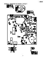
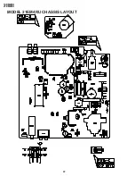
Страница 21: ...21 14EM4RU 21EM4RU MODEL 14EM4RU CHASSIS LAYOUT ...
Страница 22: ...22 14EM4RU 21EM4RU MODEL 21EM4RU CHASSIS LAYOUT ...
Страница 23: ...23 14EM4RU 21EM4RU BLOCK DIAGRAM CRT UNIT BLOCK DIAGRAM 14EM4RU CRT UNIT BLOCK DIAGRAM 21EM4RU ...
Страница 24: ...24 14EM4RU 21EM4RU BLOCK DIAGRAM MAIN UNIT 14EM4RU ...
Страница 25: ...25 14EM4RU 21EM4RU ...
Страница 26: ...26 14EM4RU 21EM4RU BLOCK DIAGRAM MAIN UNIT 21EM4RU ...
Страница 27: ...27 14EM4RU 21EM4RU ...
Страница 28: ...28 14EM4RU 21EM4RU BLOCK DIAGRAM HEADPHONE UNIT BLOCK DIAGRAM ...
Страница 30: ...30 14EM4RU 21EM4RU A B C D E F G H I J 1 2 3 4 5 6 7 8 9 10 MAIN UNIT 14EM4RU SCHEMATIC DIAGRAM ...
Страница 31: ...31 14EM4RU 21EM4RU 10 11 12 13 14 15 16 17 18 19 ...
Страница 32: ...32 14EM4RU 21EM4RU MAIN UNIT 21EM4RU A B C D E F G H I J 1 2 3 4 5 6 7 8 9 10 ...
Страница 33: ...33 14EM4RU 21EM4RU 10 11 12 13 14 15 16 17 18 19 ...
Страница 34: ...34 14EM4RU 21EM4RU A B C D E F G H I J 1 2 3 4 5 6 7 8 9 10 CRT UNIT 14EM4RU CRT UNIT 21EM4RU ...
Страница 35: ...35 14EM4RU 21EM4RU A B C D E F G H I J 1 2 3 4 5 6 7 8 9 10 HEADPHONE UNIT ...
Страница 37: ...37 14EM4RU 21EM4RU 10 11 12 13 14 15 16 17 18 19 ...
Страница 38: ...38 14EM4RU 21EM4RU PWB A MAIN UNIT Chip Parts Side A B C D E F G H I J 1 2 3 4 5 6 7 8 9 10 ...
Страница 39: ...39 14EM4RU 21EM4RU 10 11 12 13 14 15 16 17 18 19 ...
Страница 49: ...49 14EM4RU 21EM4RU ...


