background image

Hardware Manual PCD1.M0160E0 │ Document 27-622

 | 

Version ENG04 │ 2018-08-20

Saia-Burgess Controls AG

System ressources

CPU / Control Process Unit

3-7

3

3.5.4 

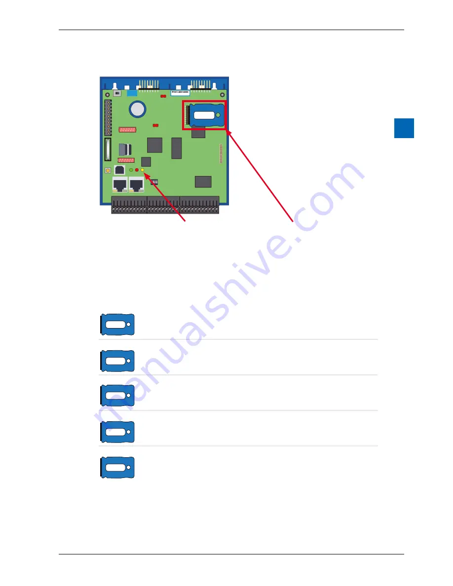
Flash Memory Module PCD7.R5xx for file system

PCD7.R5xx


Flash card status LED (yellow) switches on when the permanent flash memory 

extensions.

The flash card is inserted directly into the main circuit board. A screw in the cover 

secures the flash card in place. The mechanical cover is designed so that the flash 

card cannot loosen from the slot due to vibrations.

Memory Modules for PCD1.M0_ CPU

PCD7.R550M04

Flash memory module with file system Enables the saving of files, such 

as those for the webserver. The PCD can access the files directly through the 

FTP or HTTP server and write all PC-readable files (*.csv) directly to the mod

-

ule.

PCD7.R560

BACnet firmware module for slot M1

PCD7.R562

BACnet firmware module for slot M1 


with 128 MB for program storage and file system

PCD7.R580

Lon over IP firmware module for slot M1

PCD7.R582* 

Lon over IP firmware module for slot M1 


with 128 MByte for program storage and file system

Содержание PCD1.M0160E0

Страница 1: ...Document 27 622 Version ENG02 2018 08 20 Hardware Manual for the PCD1 M0160E0 ...

Страница 2: ...rdware version number 3 3 3 4 Firmware Version for the PCD1 M0_ COSinus update 3 4 3 5 System memory structure 3 5 3 5 1 Memory management of the PCDs with COSinus operating system 3 5 3 5 2 Flash Memory Structure on PCD1 M0_ 3 6 3 5 3 On Board Memory for the File System 3 6 3 5 4 Flash Memory Module PCD7 R5xx for file system 3 7 3 6 System resources 3 8 3 6 1 Program Blocks 3 8 3 6 2 Data Types V...

Страница 3: ...5 5 2 1 PCD7 F110S Serial Interface Module RS 485 RS 422 5 7 5 2 2 PCD7 F121S Serial Interface Module RS 232 5 8 5 2 3 PCD7 F150S Serial Interface Module RS 485 5 9 5 2 4 PCD7 F180S Serial Interface Module Belimo MP Bus 5 10 6 Configuration 6 1 Requirements 6 1 6 2 General Information 6 1 6 3 Running the Device Configurator 6 2 6 4 Media Mapping for Digital Inputs on board 6 4 6 5 Media Mapping fo...

Страница 4: ...r 4 1 1 and 6 1 3 PGND connection on terminal X3 Pin 37 Chapter 4 3 New PCD7 W600 for Slot A typo corrected EN03 2014 11 19 2015 02 10 2015 03 10 2015 03 10 5 3 Modbus also for Port 0 Dimensions for screw mounting Various corrections ENG04 2016 05 25 2018 08 20 2016 05 25 2018 08 20 3 9 Watchdog Connection example 4 1 2 Interrupt Connection 4 1 4 Digi I O Connection diagram 4 1 6 Interrupt Device ...

Страница 5: ... the document The numbers separated by dots indicate the relevant chapter numbers M1 SlotA Slot for memory module 3 7 COSinus Operating system and automation server 3 4 Terminals for integrated inputs and outputs 4 1 1 Terminating resistance RS 485 5 3 Battery 2 3 Slot optional serial interface for communication 5 4 Supply voltage 2 4 Watchdog 3 8 On board RS 485 interface 5 3 USB PGU connection 5...

Страница 6: ...recommend the following documentation on the topics Topic Documentnumber Language Version and Title System catalogue 26 215_ENG Programming tools Saia PG5 26 732_ENG Programming 26 733_ENG Ethernet TCP IP 26 776_ENG RS 485 Network 26 740_ENG A wealth of information is available on the support homepage Support www saia support com PCD Homepage www saia pcd com ...

Страница 7: ...oftware configuration maintenance and troubleshooting are covered in the respective sections 2 1 1 Instructions for connecting Saia PCD controllers to the internet When Saia PCD controllers are connected directly to the internet they are also a potential target of cyber attacks For secure operation appropriate pro tective measures must always be taken PCD controllers include simple built in protec...

Страница 8: ... earthing cable by the shortest route The shielding is normally only connected to the control cabinet on one side unless the available potential equalisation has a significantly lower resistance than the shielding resistance Inductive loads installed in the control cabinet e g protective coils must be equipped with suitable suppressors RC elements Control cabinet components with high field strengt...

Страница 9: ...ll element addresses in the PCD family start from 0 Addressing the inputs or outputs via Saia PG5 The CPU s on board inputs and outputs can be assigned to flags and registers media mapping by the programmer using the Device Configurator Device Con figurator in the Saia PG5 tool If IOs are media mapped these IOs cannot be reached directly from the program Further details about the programming can b...

Страница 10: ...imensions in mm W x H x D 142 x 142 x 61 2 2 2 Mounting Position and Ambient Temperature Module holders are normally mounted on a vertical surface in which case I O connections to modules are also vertical With this mounting position an ambient temperature between 0 C and 55 C is permissible Vertical mounting should be preferred All other positions are less favourable to air circulation so their a...

Страница 11: ...he housing against the top hat rail and snap into the rail causing the springs to give way under the counter pressure 4 Press the PCD down on the upperedge of the top hat rail and pull on it gently in order to ensure that the PCD is securely engaged 5 For removal of the cover see chapter 2 2 5 Installation Instructions and Recommendations Installation in Power Distribution Unit The PCD1 M0160E0 me...

Страница 12: ...yet mounted 1 Hold the PCD1 so that the label reads upside down The I O connections are now at the top 2 Next rotate the PCD1 until one of its two housing sides is in view 3 Holding the bottom edge of the housing cover with the fingertips of one hand and the I O connections in the fingers of the other hand carefully pull on both parts housing cover and lower part of PCD1 to separate them PCD1 is m...

Страница 13: ...ng mounting instructions assume that the PCD is to be mounted on a wall in front of the person performing the installation 100 104 20 Two holes in the base plate for fastening the controller These two screws cannot be tighten they are covered by the print 1 Remove housing cover as described under 2 2 5 2 Install all four round head screws according to mounting dimensions Screw them down far enough...

Страница 14: ...ck up battery CPU model Battery Buffer time PCD1 M0_ Renata CR2032 lithium battery 1 3 years1 1 The higher the ambient temperature the shorter the buffer time CPUs with lithium batteries are not maintenance free The battery voltage is monitored by the CPU If the battery voltage is 2 4 V or the battery is absent the CPU attempts to start the XOB2 If this is not included in the program the ERROR LED...

Страница 15: ...hielding plate in the PCD1 housing form a reliable multiple contact point with the module The zero potential minus of the 24 VDC supply is connected to the minus terminal of the supply This should be connected to the earthing rail using the shortest possible cable 25cm with a cross section of 1 5 mm2 Any shielding of analogue signals or communications cables should take place either through a minu...

Страница 16: ...nterfaces Programming interface USB 3 Optional serial data interface Port 1 to Slot A 1 PCD7 F1xxS module RS 232 RS 422 485 MP Bus or Bluetooth Port 0 RS 485 X3 terminal block up to 115 kbit s Profi S Net interface DP slave Port 0 up to 187 5 kbps Ether S Net interface 2 Port Switch Field bus connections Serial S Net Profi S Net Profibus DP slave 1 The specified time period is a buffer time which ...

Страница 17: ... 5 13 2 Hz constant amplitude 1 42 mm 13 2 150 Hz constant acceleration 1 g Electrical safety Protection type IP20 in accordance with EN60529 Air leak paths In accordance with EN61131 2 and EN50178 Between circuits and housings and between electrically isolated circuits Overvoltage category II Pollution severity 2 Test voltage 350 V 50 Hz AC rated unit voltage 24 VDC Electromagnetic compatibility ...

Страница 18: ...elease a product undergoes improvements and modifications in subsequent years In order to be able to recognise such modifications there is a so called hardware version number Based on this number the user can check whether a function is provided depending on the hardware This can be viewed with the Saia PG5 Online Configurator under Hardware Info or on the label on the back side of the PCD1 ...

Страница 19: ... cable modem USB Ethernet A modem connection is never permitted Modems can block so that remote access is no longer possible In these cases it is necessary to visit the system in person Other connection options are preferred Open the online configurator and go offline In the Tools menu select Update Firmware and use the Browse function to select the path for the file with the new firmware version ...

Страница 20: ...rnal battery buffered RAM memory Controllers such as Saia PCD3 Mxx60 Saia PCD1 M0 _ M2_ and the programmable Web Panel MB are equipped with an on board backup memory Flash When downloading an user application with Saia PG5 all necessary files are also stored on request in this backup memory PG5 default setting If the power supply is connected to the controller and there is no executable program in...

Страница 21: ...tory of an SD flash card 3 5 2 Flash Memory Structure on PCD1 M0_ File system for the user Primarily used for BacNet PLC file system only for FW The end user cannot access this partition Used for linked web projects web builder 3 5 3 On Board Memory for the File System To use the on board flash memory select PCD Memory Internal The internal flash memory has the following name INTFLASH The absolute...

Страница 22: ...signed so that the flash card cannot loosen from the slot due to vibrations Memory Modules for PCD1 M0_ CPU PCD7 R550M04 Flash memory module with file system Enables the saving of files such as those for the webserver The PCD can access the files directly through the FTP or HTTP server and write all PC readable files csv directly to the mod ule PCD7 R560 BACnet firmware module for slot M1 PCD7 R56...

Страница 23: ...rogram elements Exception system dependent organisation blocks XOB 64 0 63 Called from the system Program Blocks PB 1000 0 999 Subprograms Function blocks FB 2000 0 1999 Subprograms with parameters Sequential blocks SB a total of 6000 steps and transitions 96 0 95 Sequential processes for Graftec programming Bloc structure FB 999 1999 PB 299 999 COB 15 31 COB COB 0 XOB 31 31 XOB XOB 0 PB PB 0 FB F...

Страница 24: ...umber Addresses Comments Flags 1 bit 16 384 F 0 16 383 Flats are not transient but a transient range starting from Address 0 can be configured Register 32 bit 16 384 R 0 16 383 For integer or floating point values Text data blocks 8191 X or DB 0 8190 For text and DB Timer counter 31 bit 16001 T C 0 1599 The breakdown of timers and counters can be configured Timers count down periodically under the...

Страница 25: ...al Run status A condition was set in the debugger Run until which has not been fulfilled yet Run with error The same as Run but with an error message Run conditional with error The same as Run conditional but with an error message Stop The status Stop occurs in the following cases Programming unit connected in PGU mode while the CPU was switched on PGU stopped by programming unit Condition for BED...

Страница 26: ...sent battery In the process media resources flash registers flags etc user program and hardware settings are deleted The time is set to 00 00 00 01 01 1990 The backup of the on board flash is NOT deleted Red blinking slowly 2 Hz The PCD does not start up and switches to Stop mode Red Green blinking 2 Hz Saved data is deleted which means media resources flash registers flags etc user program hardwa...

Страница 27: ...30 D D PCD1 M0160E0 Main switch Process e g Output modules Danger observe the contact load of the WD relay Possibly via power contactor WD Relay Watchdog Relais Power dangerous outputs Functional description As soon as the watchdog relay is called at the address O 255 by a switch on off frequency of 200 ms the relay contact closes It remains closed until the pulse time exceeds 200 ms If this happe...

Страница 28: ...or 1 15 0 STL WD_Flag Helpsflag invers OUT WD_Flag OUT O 255 Output 255 blinking ECOB With this code the watchdog triggers even for continuous loops that are due to programming Regarding user program cycle time please note the following With cycle times longer than 200 ms the code sequence must be repeated multiple times in the user program in order to prevent the watchdog triggering during RUN Si...

Страница 29: ...hen be output at least every 200 ms otherwise the watchdog will be triggered and the PCD restarted Instruction in IL code Label Com mand Operand Comment SYSWR K 1000 Software watchdog instruction R K x Parameter according to the following table K Constants or R Register Blank space x 0 The software watchdog is deacti vated x 1 The Software Watchdog is activat ed if the instruction is not repeated ...

Страница 30: ...BACnet LON etc Data for the initialisation of resources for the first time Build or Rebuild All 2 Program download Download in the SPM opens the window opposite If all settings are as desired see below the user program is loaded into the PLC with the Download button 3 Options area Download First time Initialisation Data Initialisation of media registers flags etc for the first time Clear Media R F...

Страница 31: ...rses the file and performs a restart The PLC switches to STOP for the parsing of the new file This step takes 2 to 5 seconds depending on the size of the user program 5 After download area Run the program Sets the PLC to RUN once the download is successfully completed Stay in Stop After the download PLC remains in STOP 6 Backup to Flash area Backup to on board flash Physical outputs with or withou...

Страница 32: ...D already contains another program Behaviour area Download automatically after successful build Download program only if changed Go online after successful download observation mode It is not possible to download only those blocks which have been modified The user program is downloaded into the on board memory in a file and after a restart of the system the process is complete If the download is n...

Страница 33: ... on board flash memory is backed up in the folder PLC_SYS This folder is not visible for the user Access is not permitted Registers flags timer and counters are not saved in this manner During a restore the text DB data is copied back into the SRAM memory Backup to the INTFLASH file system In order to be able to use backup restore with internal flash a PCD_ BACKUP folder must be created RAM DB tex...

Страница 34: ...nd When using use of the backup function to M1 modules no other files should be written to the module M1 FLASH PCD_BACKUP sbak PCD1 1 PCD1 2 Please note that a 512 kByte user program and 128 kByte RAM DB text will generate a file of approximately the same size Limitations Files generated cannot be copied directly from one folder to another These files may not be deleted from the original folder or...

Страница 35: ... options are available With the PG5 under Online Flash memory Restore source of flash or By pressing the Run Stop button for at least 3 5 seconds in RUN mode ATTENTION If the button is pressed for longer than 10 seconds there is the risk of resetting the system and or deleting the memory The CPU searches memory locations for backup files in the following order 1 M1 Flash 2 INTFLASH 3 PLC_SYS ...

Страница 36: ...Outputs I O 4 1 4 4 Inputs and Outputs This chapter describes the inputs and outputs of the PCD1 M2_ in terms of their function and pin assignment Three possible locations for inputs and outputs are described Optional extension can be use external RIOs 4 1 On Board On board means mounted on the CPU mother board ...

Страница 37: ...2 14 In 3 Input 3 15 IX0 Interrupt or Input 16 IX1 Interrupt or Input 17 AGND 18 AIN0 Analogue Input 0 19 AIN1 Analogue Input 1 X2 PCD7 F121S PCD7 F110S PCD7 F180S PCD7 F150S PCD7 W600 RS 232 RS 485 RS 422 Belimo RS 485 isol 4xAO 0 10V 20 PGND PGND PGND PGND PGND PGND 21 TxD Rx Tx Tx MP Rx Tx A0 22 RxD Rx Tx Tx MFT Rx Tx A0 23 RTS Rx IN A1 24 CTS Rx A1 25 PGND PGND PGND PGND PGND PGND 26 DTR RTS A...

Страница 38: ...otection No LED No Terminals Plug in screw terminal block 11 12 13 14 15 16 17 18 19 10 9 8 7 6 5 4 3 2 1 0 I2 I3 I1 I0 O0 O2 O3 O1 IO5 IO4 IO6 IO7 X0 X1 U ext GND IX0 IX1 AI0 AI1 24 VDC 3 6 mA In3 digital inputs PWO or O8 The terminals No 15 and No 16 can be used as an input or as an interrupt see Section 4 1 7 Int1 11 12 13 14 15 16 17 18 19 10 9 8 7 6 5 4 3 2 1 0 I2 I3 I1 I0 O0 O2 O3 O1 IO5 IO4...

Страница 39: ...mber of outputs 4 Voltage range 24 VDC 12 32 VDC smoothed Output current Max 0 5 A Output delay typ 50 µs max 100 µs at ohmic load Contact protection Transistors LEDs No Connections Plug in screw terminal block 11 12 13 14 15 16 17 18 19 10 9 8 7 6 5 4 3 2 1 0 Uext Out0 I2 I3 I1 I0 O0 O2 O3 O1 IO5 IO4 IO6 IO7 X0 X1 Uext GND IX0 IX1 AI0 AI1 24 VDC current Limit PWO or O8 Digital outputs ...

Страница 40: ...ured as an output Short circuit protection Yes Voltage range 24 VDC 12 32 VDC smoothed Output current Max 0 5 A Output delay Typ 50 µs max 100 µs at Ohmic load LEDs No Connections Plug in screw terminal block Uext Uext Uext 11 12 13 14 15 16 17 18 19 10 9 8 7 6 5 4 3 2 1 0 I2 I3 I1 I0 O0 O2 O3 O1 IO5 IO4 IO6 IO7 X0 X1 Uext GND IX0 IX1 AI0 AI1 24 VDC 3 6 mA In7 Uext Out7 In6 In5 In4 Out6 Out5 Out4 ...

Страница 41: ... as a normal digital output or as a PWM output Configuration takes place in the Device Configurator There is an FBox for the using of the PWM output Number of PWM outputs 1 Voltage range 24 VDC 12 32 VDC smoothed Output current Max 0 2 A Adjustable frequencies 1 Hz 4 Hz 15 Hz 30 Hz 61 Hz 122 Hz 244 Hz 488 Hz 975 Hz 1950 Hz Duty cycle range 0 100 Terminal Plug in screw terminal block Maximum operat...

Страница 42: ... Controls AG On board PWM Output Inputs Outputs I O 4 7 4 11 12 13 14 15 16 17 18 19 10 9 8 7 6 5 4 3 2 1 0 Uext PWM Out8 I2 I3 I1 I0 O0 O2 O3 O1 IO5 IO4 IO6 IO7 X0 X1 Uext GND IX0 IX1 AI0 AI1 24 VDC PWM Output current Limit PWO or O8 t T PWM Output time Frequency 1 T Duty Cycle t T ...

Страница 43: ... as short as possible so that sufficient time remains between the interrupts in order to process the rest of the user program Many FBoxes are intended for cyclical calling and are not suitable for use in XOBs or are only suitable to a limited extent Exception The FBoxes of the Graftec family standard library are well suited PCD1 Interrupt Inputs 24 VDC Both interrupt inputs are located on the main...

Страница 44: ...ed as follows PG5 Device Configurator Î Î Onboard In Outputs Î Î Properties Î Î Interrupts Operation IX0 also applies for IX1 With a positive flank at Input IX0 XOB 20 is called The maximum reaction time until the call of XOB 20 is 1 ms The code in this XOB defines how the system should react to the events e g by increment a counter max input frequency 1 kHz whereas the pulse pause ratio is 1 1 ma...

Страница 45: ... Ω Input filter typ 5 ms Input range for temperature sensors PT1000 50 400 C NI1000 60 200 C NI1000 L S 30 140 C Resistance 0 2 5 kΩ Precision at 25 C 0 5 Temperature sensor 0 55 C 0 25 Overload protection 10 V Range 35 V 39 V TVS diode 20 mA Range 40 mA LED No Terminals Plug in pressure 10 pin terminal block 3 5 mm for wiring up to 1 mm2 On delivery preconfigured for NI1000 Configuration of the a...

Страница 46: ... C 500 1400 Limits 300 1400 Each time the min max values are reached the min max status flag is set Resistance voltage and current inputs The overall value range is defined by the range type Model min max Status flag Range of the calculated values Resistance 0 2500 Ω 0 25000 Min Flag not set Limit exceeded 25500 25000 2 Voltage input 10 10 V Xx yy 102 of the defined range Current input 20 20 mA Xx...

Страница 47: ... I2 I3 I1 I0 X1 IX0 IX1 AI0 AI1 O0 O2 O3 O1 IO5 IO4 IO6 IO7 X0 Uext GND Pt 1000 Ni 1000 Resistance PWO or O8 10 10 VDC 0 20 mA Connection concept for two wire transmitters 11 12 13 14 15 16 17 18 19 10 9 8 7 6 5 4 3 2 1 0 4 20 mA 0 20 mA δ υ I2 I3 I1 I0 O0 O2 O3 O1 IO5 IO4 IO6 IO7 X0 X1 Uext GND IX0 IX1 AI0 AI1 24 VDC PWO or O8 4 20 mA through the user program or in the Saia PG5 Device Configurato...

Страница 48: ...rdungsschiene General specifications Technical data Module compatibility PCD1 M2xxx PCD1 M0160E0 PCD1 M2110R1 Module current consumption V 25 mA 5 V 30 mA Number of outputs 4 Terminals 1 plug in screw terminal block 10 pole 3 5 mm for wiring up to 1 mm2 Isolation No isolation between channels and or PCD Output signal range resolution With D A converter 12 bits Nominal range 0 10 V Resolution 2 6 m...

Страница 49: ...full range change 5 ms Overshooting 0 1 of the full scale 10 V Scaling PG5 0 4095 0 10000 or user defined Prerequisite PCD firmware version 1 23 39 or higher PG5 version 2 1 300 or higher Programming with media mapping When the media mapping is enabled each module has these following registers The analogue values shall be directly written in the AnalogueOutputx registers Each channel will be updat...

Страница 50: ...PW commands Here an IL program example to write an analogue value to the output0 and to read the diagnose register With direct access it is possible to know which channel has not been correctly updated if the status register is read direct after the Write command Bit Status Description 0 1 if a communication error has been detected between PCD and module This bit is automatically cleared when the ...

Страница 51: ... permantly activated if media mapping is used or Shortly blink with direct access Module detection If the module is not plugged there is a history entry If you need to detect if the module is plugged or not in your program code you can use the following function If the module has been correctly plugged the status value is a positive num ber and all device information can be read If the module has ...

Страница 52: ...ules Integrated webserver for diagnostics support and commissioning connection to PC via optional PCD3 K225 connection cable PCD model Max number of PCD3 I O PCD3 T760 RIO nodes 256 per node PCD3 RIOs are used to detect decentral I O signals PCD3 RIOs can communicated with all master PCD via Profibus DP this can take place through the integrated Profi S I O on the PCD1 M2_ A detailed description i...

Страница 53: ...cations interface for the purpose of simplification Using the SBCS Bus SBC S Bus stands for the proprietary communications protocol of Saia PCD The SBC S Bus is basically designed for communications using the engineering and debugging tools as well as for connection to management levels process control systems It is not suitable or approved for connecting the field devices of other manufacturers A...

Страница 54: ...12 Mbps with Softconnect Protection transil Hardware On board USB 5V supply The USB port is only used as a PGU interface To use the USB interface the program package Saia PG5 version 2 0 or later must be installed on the PC If the PCD is connected to the PC for the first time through the USB port the PC operating system Windows automatically loads the corresponding Saia PCD USB driver To connect t...

Страница 55: ...9 A new 10 100 Mbits switch which automatically adapts to the two speeds is used for these Ethernet connections Both sockets can be used independently of one another ETH1 ETH2 Function 2 port switch Jack type 2 RJ45s vertically positioned metal housing 2 LEDs each Meaning of the LEDs per jack Orange LED Link connection and activity Green LED Speed Off 10Mbits On 100 Mbits ...

Страница 56: ... Switch S1 connecting or disconnecting the RS 485 termination resistors With switch S1 the terminating resistors are switched on or off Switch S1 must be set to C closed at both outer stations For all other stations switch S1 remains in the position O factory setting Schematic diagram of an RS 485 bus with terminating resistors 5 V RX TX n n 39 n n n n 38 RX TX 5 V Pull up 330 Ohm Termination Resi...

Страница 57: ...ck X2 connection terminals for Slot A Older interface modules without S at the end of the product designation e g PCD7 F110 are not compatible with PCD1 M0_ Overview of the interface types PCD7 F1xxS with housing 2012 or later PCD7 F1xxS previous design PCD7 F1xx not compatible with PCD1 M2_ Important PCD7 F1xxS devices with hardware version A are not compatible with earlier PCDs PCD1 M1xx PCD2 M1...

Страница 58: ... hardware version A are used with the following devices the interface modules will become hot and their correct function cannot be guaranteed PCD1 M1xx PCD2 M1xx PCD2 M48x PCS The hardware version can be seen on the white label of a PCD7 F1xxS module in the middle text line Solution Only use PCD7 F1xxS interface modules PCD7 F1xxS with hardware version B or newer These are suitable for all PCD gen...

Страница 59: ...N C O Open not terminated factory setting Plug assignment RS 485 Bus cable PCD1 M0_ Terminal Block X2 peripheral Strands twisted and shielded RX TX RX TX PGND RX TX RX TX PGND PGND 20 21 22 23 24 25 26 27 28 29 Strands twisted and shielded RS 422 Bus cable PCD1 M0_ Terminal Block X2 peripheral DTE 20 21 22 23 24 25 26 27 28 29 PGND TX TX PGND PGND RX RX RTS RTS CTS CTS TX TX PGND RX RX RTS RTS CTS...

Страница 60: ...n PCD7 F121S Standard Cabling RS 232 Bus cable PCD1 M0_ Terminal Block X2 peripheral D Sub m 9 pole D Sub w 25 pole 20 21 22 23 24 25 26 27 28 29 PGND TXD RXD PGND PGND RTS CTS DTR DSR COM DCD TXD RXD PGND RTS CTS DTR DSR COM DCD 3 2 5 7 8 4 6 1 2 3 7 4 5 20 6 8 Cabling for Modem connection RS 232 Bus cable PCD1 M0_ Terminal Block X2 20 21 22 23 24 25 26 27 28 29 PGND TXD RXD PGND PGND RTS CTS DTR...

Страница 61: ...overvoltage with an anti surge diode 10 V Termination resistors can be connected CLOSED or disconnected OPEN with a jumper PCD7 F150S RS 485 termination Gate 1 2 ON C O Close terminated Gate 1 2 ON C O Open not terminated factory setting Cabling RS 485 Bus cable PCD1 M0_ Terminal Block X2 peripheral Strands twisted and shielded RX TX RX TX PGND RX TX RX TX PGND PGND SGND 20 21 22 23 24 25 26 27 28...

Страница 62: ...Terminal Block X2 24 VDC MP MFT PGND PGND IN GND 20 21 22 23 24 25 26 27 28 29 Cabling MP Bus device 20 PGND Earth connection MP string 21 MP Multi Point The MP bus is the Belimo master slave bus Up to 8 slaves can be attached to one master device They are MFT 2 flap drives MFT 2 valve drives MFT fire protection flap drives VAV compact controller NMV D2M 22 MFT MFT programming device MP bus intern...

Страница 63: ...l Information This chapter describes how the Saia PG5 Device Configurator is used The Device Configurator defines cyclical media mapping in order to enable a link between peripheral I O module values and the device resources e g PCD flags and registers direct access to programming instructions for reading values from and transmitting values to the peripheral input module For the PCD1 M0_ I O handl...

Страница 64: ...tion Configuration Device Configurator 6 2 6 6 3 Running the Device Configurator Um HW Konfiguration Protokolleinrichtung und E A Behandlung einzurichten ist der De vice bzw Gerätekonfigurator zu verwenden The Device Configurator is started by double clicking on the Device Configurator symbol in the project directory tree ...

Страница 65: ...nt 27 622 Version ENG04 2018 08 20 Saia Burgess Controls AG Device Configurator Configuration Device Configurator 6 3 6 Help Help for the Device Configurator can be found under Help Topics in the Help menu Click on one of the Help topics ...

Страница 66: ...apping Configuration Device Configurator 6 4 6 6 4 Media Mapping for Digital Inputs on board The media mapping of digital inputs uses 16 flags Mapping table for digital inputs 6 5 Media Mapping for Digital Outputs on board The media mapping of digital outputs uses 16 flags Mapping table for digital outputs ...

Страница 67: ...ns PG5 Device Configurator for PCD1 M0160_ Select whether channel 4 to 7 should be used as a digital input or output Select whether the PWM channel should be used as a PWM output or standard output Select whether the watchdog channel should be used as a watchdog output or standard relay output Select whether the interrupt channels should be used as interrupts or standard digital inputs ...

Страница 68: ...22 Version ENG04 2018 08 20 Saia Burgess Controls AG Special functions analogue inputs Configuration Device Configurator 6 6 6 6 7 Analogue inputs Properties Mapping setup for values and status or diagnosis Channel setup and scaling information ...

Страница 69: ...0160E0 Document 27 622 Version ENG04 2018 08 20 Saia Burgess Controls AG Special functions analogue inputs Configuration Device Configurator 6 7 6 Mapping table for analogue inputs Mapping table for status of analogue inputs ...

Страница 70: ... and to enable the hardware clock if present to carry on running PCD1 devices are equipped with a back up battery CPU model Buffer Buffer time Image PCD1 M0_ Renata CR 2032 lithium battery 1 3 years1 1 Depending on the ambient temperature the higher the temperature the shorter the buffer time Battery voltage is monitored by the CPU If the battery is absent or capacity is lost battery voltage less ...

Страница 71: ...t the Renata CR 2032 button battery with the label side pole up slightly pushing the battery retaining clip to the side The symbol can also be seen on the circuit board Fit the housing cover Check the battery display red LED dark Battery o k yellow triangular LED dark Batteryfailer yellow triangular LED blinking Hardware Manual PCD1 M0160E0 Document 27 622 Version ENG04 2018 08 20 Saia Burgess Con...

Страница 72: ...ing into contact with electrical components you should at least touch the system s negative pole cabinet of PGU connector However it is better to use a grounding wrist strap with its cable permanently attached to the system s negative pole This sign accompanies instructions that must always be followed Explanations beside this sign are valid only for the SBC PCD Classic series Explanations beside ...

Страница 73: ... CTS Clear to send Readiness to send DTR Data terminal ready Terminal ready DSR Data set ready Ready for use RI Ring indicator Incoming call DCD Data carrier detect Partner ready Signals to RS 232 Signal type Logic status Setting Setpoint value Data signal 0 empty 1 character 3 V to 15 V 15 V to 3 V 7 V 7 V Control message signal 0 off 1 on 15 V to 3 V 3 V to 15 V 7 V 7 V Hardware Manual PCD1 M016...

Страница 74: ...ssage signal 0 off 1 on RTS positive to RTSRTS positive to RTS RS 485 Signal type Logic status Polarity Data signal 0 empty 1 character RX TX positive to RX TX RX TX positive to RX TX Not all manufacturers use the same connection configuration Therefore it may be necessary to cross the data lines In order to ensure fault free operation of an RS 485 network the network should be closed at both ends...

Страница 75: ...s and registers Modules Carrier cards for input output electronics Module holder CPU LIO or RIO devices which can accommodate the aforementioned modules Motherboard Main circuit board CPU IL Instruction list PCD program code NT New technology means the PCD generation following the first generation On board means mounted on the CPU circuit board Parsing A parser is often a type of compiler which ch...

Страница 76: ...ation of the clock after a power supply shut down terminated Reflections at the line ends are prevented through line termination PCD2 M2xxx x in the product designation stands for a number 0 9 In this case it is a three digit number such as PCD2 M2110 Hardware Manual PCD1 M0160E0 Document 27 622 Version ENG04 2018 08 20 Saia Burgess Controls AG ...

Страница 77: ...pport saia pcd com Supportsite www sbc support com SBC site www saia pcd com International Represetatives SBC Sales Companies www saia pcd com contact Postal address for returns from customers of the Swiss Sales office Saia Burgess Controls AG Service Après Vente Bahnhofstrasse 18 3280 Murten Switzerland Hardware Manual PCD1 M0160E0 Document 27 622 Version ENG04 2018 08 20 Saia Burgess Controls AG...

Отзывы: