– 3 –
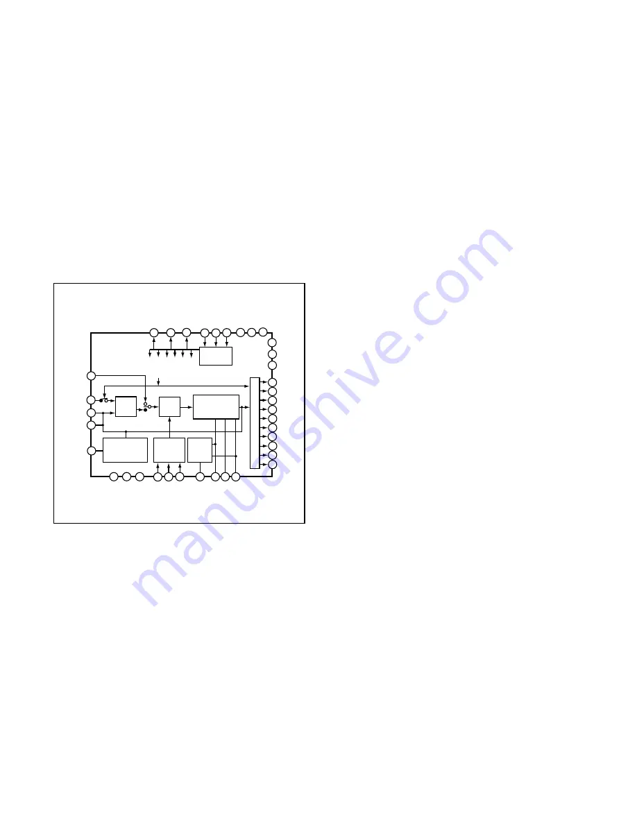
Fig. 1-2. IC905 Block Diagram
3. IC904 (V Driver)
V driver is necessary in order to generate the clocks (vertical
transfer clock, horizontal transfer clock and electronic shutter
clock) which driver the CCD.
IC904 is V driver. In addition the XV1-XV4 signals which are
output from IC101 are the vertical transfer clocks, and the
XSG signal which is output from IC102 is superimposed onto
XV1 and XV3 at IC904 in order to generate a ternary pulse.
In addition, the XSUB signal which is output from IC101 is
used as the sweep pulse for the electronic shutter.
4. IC905 (CDS, PGA, A/D Converter and H driver)
The video signal which is output from the CCD is input to Pin
(51) of IC905. There are inside the CDS block, PGA block
and A/D converter block.
The setting of sampling phase and PGA is carried out by se-
rial data at Pin (63) of IC935. The video signal is carried out
A/D converter, and is output by 10-bit. A H driver is inside
IC905, and H1, H2 and RG clock are generated at IC905.
5. Lens drive block
5-1. Iris drive
When the drive signals (IIN+ and IIN–) which are output from
the ASIC (IC101), it is driven by the driver (IC951), and are
then used to drive the iris steps.
5-2. Focus drive
When the drive signals (FIN_A, FIN_-A, FIN_B and FIN_-B)
which are output from the ASIC expansion I/O port (IC105),
the focus stepping motor is driven by the driver (IC951). De-
tection of the standard focusing positions is carried out by
means of the photointerruptor (FOCUS PI) inside the lens block.
5-3. Zoom drive
When the drive signals (ZIN+ and ZIN–) which are output from
the ASIC (IC101), the zoom motor is driven by the driver
(IC951). Detection of the standard zoom positions is carried
out by means of photointerruptor (ZOOM PI and PI2) inside
the lens block.
5-4. Shutter drive
When the drive signals (SIN+ and SIN–) which are output from
the ASIC (IC101), it is driven regular current by the driver
(IC951).
VRB
D9
D8
D7
D6
D5
D4
D3
D2
D1
D0
Reset
DV
SS
AV
SS
VRM
VRT
BIAS
CDS_CS
SDATA
SCK
DLL_C
MON
ID
BLKFB
BLKC
BLKSH
CDS_in
ADC_in
DRDV
DD
DV
DD
AV
DD
CLK_in
HD_in
VD_in
RG
H1A
H2A
TIMING
generator
Serial
interface
Bias
genera-
tion
DC offset
compensation
ciruit
10 bit
ADC
PGA
CDS
PBLK
CPDM
CPOB
ADCK
SP2
SP1
Output latch circuit
Содержание Xacti VPC-S1
Страница 25: ......
Страница 26: ...Aug 03 SANYO Electric Co Ltd Osaka Japan ...


