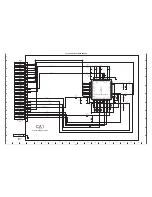
C2
NOTES:
1. All resistance values in "OHMS" unless otherwise noted.
(K=1,000 ; M=1,000,000)
2. All capacitance values in "µF" unless otherwise noted.
p=pico farad ; n=nano farad ; µ ,u or U=micro farad
3. All inductance values in "µH" unless otherwise noted.
µ ,u or U=micro henry ; m=milli henry
PRODUCT SAFETY NOTICE
THE COMPONENTS DESIGNATED BY A SYMBOL ( ) IN THIS
SCHEMATIC DIAGRAM DESIGNATES COMPONENTS WHOSE VAL-
UE ARE OF SPECIAL SIGNIFICANCE TO PRODUCT SAFETY.
SHOULD ANY COMPONENT DESIGNATED BY A SYMBOL NEED TO
BE REPLACED, USE ONLY THE PART DESIGNATED IN THE PARTS
LIST.
DO NOT DEVIATE FROM THE RESISTANCE, WATTAGE AND VOLT-
AGE RATINGS SHOWN.
EXPLANATORY NOTES (EXAMPLES)
Resistor 10K:1/16J means 10kilo ohm ±5%, 1/16watt max.
1M:1/10D means 1mega ohm ±0.5%, 1/10watt max.
(Tolerance K:±10%, J:±5%, G:±2%, F:±1%, D:±0.5%)
Capacitor 0.047:F means 0.047micro farad, Ftype.
Electrolytic capacitor
10:16 means 10micro farad, 16volt max.
Inductor 330:J means 330micro henry ±5%
470:K means 470micro henry ±10%
No description J or K means ±5%
Figure of printed wiring boards
Multilayer board:
"Side A" means the view from A side of the board.
"Side B" means the view from B side of the board.
Singlelayer board:
View from the copper-foil side of the board, otherwise noted.
PAL-H-EX
The number of "H=##" written in slant character, shows the voltage.
The number of "H=##" written in upright character, shows the height of the parts.
Содержание VPC-CA100EXBK
Страница 18: ... 18 2 6 BOARD LOCATION ST1 board TB1 board CP1 board VF1 board ...
Страница 27: ... 27 MEMO ...
Страница 29: ...2 9 Table of accessories 1 2 4 5 6 7 8 9 10 11 3 12 ...
Страница 59: ......
Страница 60: ...Jun 10 SANYO Electric Co Ltd Osaka Japan ...


