- 10 -
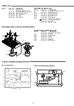
IC BLOCK DIAGRAM & DESCRIPTION
Terminal
No.
Terminal
symbols
I/O
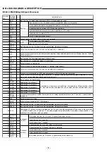
43 XVDD
-
44 XOUT
O
45 XIN
I
46 XVSS
-
47 SBSY
O
48 EFLG
O
49 PW
O
50 SFSY
O
51 SBCK
I
52 FSX
O
53 WRQ
O
54 RWC
I
55 SQOUT
O
56 COIN
I
57 *CQCK
I
58 *RES
I
59 TST11
O
60 16M
O
61 4.2M
O
62 TEST5
I
63 *CS
I
64 TEST1
I
Input terminal for reseting this LSI. Switches to "L" position for a moment at power-on.
Output terminal for test. Make sure to open circuit. (Normally "L" output)
Output terminal of 16.9344 MHz
Note: Each power terminal (VDD, VVDD, LVDD, RVDD and XVDD) must be supplyed with the same voltage.
Input terminal for test. Pull-down resistor incorporated. Make sure to ground.
Input terminal for chip selecting. Pull-down resistor incorporated. Make sure to ground when not controlled.
Input terminal for test. No pull-down resistor. Make sure to ground.
Output terminal of 4.2336 MHz
Input terminal for read/write control. Schmitt input.
Input terminal for command from micro-computer.
Input terminal either for clock to take in command input or for clock to take out sub-code from SQOUT. Schmitt inpu
Output terminal for Q output of sub-code.
Output terminal for synchronizing signals of sub-code frame. When sub-code is stood by, falls.
Input terminal for clock to read out sub-code. Schmitt input (when not used, make sure to ground.)
Output terminal for synchronizing signal (7.35 kHz) which is divided from crystal oscillator.
Output terminal for Q output standby of sub-code.
Ground terminal for crystal oscillator. Make sure to ground.
Output terminal for synchronizing signals of sub-code clock.
Monitor terminal for 1 bit or 2 bit error correction
Output terminal for sub-code P, Q, R, S, T, U or W.
DESCRIPTION
Power terminal for crystal oscillator
Joining terminal for crystal resonator (16.9344 MHz)
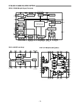
IC901 LA9241M(Servo Signal Processor)
FSS
64
63
62
61
60
59
58
57
56
55
54 53
52
51
50
49
48
47
46
45
44
43
41
40
39
38
37
36
35
34
33
42
32
31
30
29
28
27
26
25
24
23
22
21
20
19
18
17
16
15
14
13
12
11
10
9
8
7
6
5
4
3
2
1
Vcc1
LDS
LDD
BH1 PH1
LF2
VR REF1 Vcc2
DRF CE DAT CL CLK
DEF
NC
TBC
FSC
DGND
SLI
SLC
RFS-
RFSM
CV+
CV-
SLOF
HFL
TES
TOFF
TGL
JP+
JP-
SL+
SL-
SLD
SLEQ
SPD
SP-
SPG
SPI
SP
AGND
FE-
FE
FA-
FA
FD-
FD
TO
JP
TD
TD-
TA
TH
SCI
TESI
TE
TE-
TB
F
E
FIN1
FIN2
APC
RF DET
REF
VCA
I/V
BAL
VCA
INTER FACE
MICOM
SLC
RF Amp
TE
T.SERVO & T.LOGICK
F.SERVO & F.LOGICK
SPINDLE SERVO
SLED SERVO
IC902 LC78622E(Degital Signal Processor)
Содержание 164 081 00
Страница 13: ... 13 12 SCHEMATIC DIAGRAM DISPLAY This is a basic schematic diagram ...
Страница 14: ... 15 14 SCHEMATIC DIAGRAM CD This is a basic schematic diagram ...
Страница 15: ... 17 16 SCHEMATIC DIAGRAM TUNER This is a basic schematic diagram ...
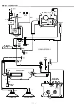
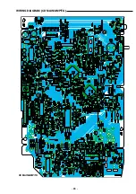
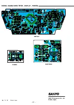
Страница 17: ... 20 WIRING DIAGRAM CD MAIN AMP TU CD MAIN AMP TU ...

