Alignment and Adjustments
4-16
Samsung Electronics
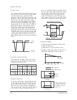
5. Output Circuit
The voltages, which are detected form an error
detection circuit of PWM IC (Differential AMP)
and Dead Time, each is applied to PWM
conparator . Due to these detection coltages, Q1,
Q2 (Output TR) parallel operate. Q482 (External
TR), however, functions as a buffer; natches
inpedance between the output port of PWM IC
and the final output TR(IRFS640). The PWM
pulse (applied to the final output FET (IRFS640
GATE) varies the IC current of high voltage
TR(Q473) by adjusting the load impedance of
starage Trans (T431). Due to this variation of
current, the gain for Q473 emitter pulse changes
T444(FBT)makes this emitter pulse became high
voltage. Such change keeps both dynamic and
static changes fixed. The output waveform of
high valtage TR emitter is as shown in the figure
below.
6. Paraneters according to beam
To maintain the set high voltage value (31kV),
parmaters such as +Ve (DC), Vcp High Voltage
change (See the table below).
7. Response Waveform
To reduce unstable high voltage fluctuation, the
existing high voltage type REG circuit controls
dynamic fluctuation by using C-block capacitor.
But, it can't detect actual dynamic fluctuation.
Also, its velocity of response to static fluctuation
is late bB power supply changes per
about 1V. A PWM modulation type REG detects
static, dynamic high voltage fluctuation for only
Ton Time (when the current of the output TR
collector flows) each 1H, and modulates the
width of PWM pulse. So, this PWM type has
better improvement in the characteristic of high
voltage REG as compared to the existing type.
8. Application Effects
1) Improvement of horizontal size fluctuation
2) Linearity improved
3) Embodiment of X-ray protection circuit
The figures below show characteristics when a
PWM high voltage REG circuit is applied.
Beam
(High voltage )
Factor of high
voltage change
Beam
(High voltage )
Width of FET
Gate Pulse
+ Ve (DC)
Vcp
High
Voltage
Parameters
High Voltage Drive Base Current
PWM Input Waveform of FET GATE
GND
GND
PWM Variation tange
Ton
Toff
Beam
High Voltage
High Voltage OFF
High Voltage REG ON
BLACK
WHITE
When a Toshiba Pattern
is recrived, the screen is
displayed as shown in
figute side
Existing type
PWM type
Содержание ST55W3PCX/XAX
Страница 10: ...Reference Information 2 4 Samsung Electronics 2 3 IC Line Up 2 3 1 Progressive ...
Страница 11: ...Reference Information Samsung Electronics 2 5 ...
Страница 12: ...Reference Information 2 6 Samsung Electronics 2 4 MICOM IIC BUS LINE UP ...
Страница 14: ...MEMO 3 2 Samsung Electronics ...
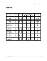
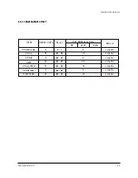
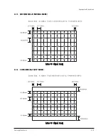
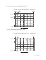
Страница 32: ...Alignment and Adjustments 4 18 Samsung Electronics 4 7 3 473W 4715W NORMAL MODE 4 7 4 473W 4715W DTV MODE ...
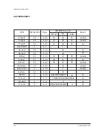
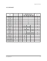
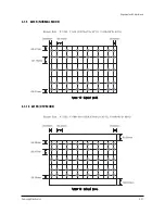
Страница 35: ...Alignment and Adjustments Samsung Electronics 4 21 4 7 9 6215R NORMAL MODE 4 7 10 6215R DTV MODE ...
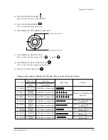
Страница 37: ...Alignment and Adjustments Samsung Electronics 4 23 4 8 Remote Control for Servicing Convergence Mode ...
Страница 52: ...MEMO 4 38 Samsung Electronics ...
Страница 56: ...MEMO 5 4 Samsung Electronics ...
Страница 86: ...TP02 TP01 10 Schematic Diagrams Samsung Electronics Schematic Diagrams 10 1 10 1 MAIN 1 TP01 TP02 ...
Страница 87: ...Schematic Diagrams 10 2 Samsung Electronics TP20 TP03 TP04 10 2 MAIN 2 TP03 TP04 TP20 ...
Страница 88: ...Samsung Electronics Schematic Diagrams 10 3 10 3 MAIN 3 TP12 TP13 TP12 TP13 ...
Страница 90: ...Samsung Electronics Schematic Diagrams 10 5 10 5 MICOM ...
Страница 91: ...Schematic Diagrams 10 6 Samsung Electronics 10 6 CRT ...
Страница 92: ...Samsung Electronics Schematic Diagrams 10 7 10 7 SUB 1 TP21 TP21 ...
Страница 93: ...Schematic Diagrams 10 8 Samsung Electronics 10 8 SUB 2 TP24 TP23 TP22 TP22 TP23 TP24 ...
Страница 94: ...Samsung Electronics Schematic Diagrams 10 9 10 9 CONVERGENCE SDC12 1 ...
Страница 95: ...Schematic Diagrams 10 10 Samsung Electronics 10 10 CONVERGENCE SDC12 2 ...
Страница 96: ...Samsung Electronics Schematic Diagrams 10 11 10 11 PRO SCAN 1 ...
Страница 97: ...Schematic Diagrams 10 12 Samsung Electronics 10 12 PRO SCAN 2 ...
Страница 98: ...Samsung Electronics Schematic Diagrams 10 13 10 13 PRO SCAN 3 ...
Страница 99: ...Schematic Diagrams 10 14 Samsung Electronics 10 14 PRO SCAN 4 ...
Страница 100: ...10 15 CG AMP Samsung Electronics Schematic Diagrams 10 15 ...
Страница 101: ...Schematic Diagrams 10 16 Samsung Electronics 10 16 AV FRONT ...
Страница 102: ...10 17 CONTROL Samsung Electronics Schematic Diagrams 10 17 ...
Страница 103: ...Schematic Diagrams 10 18 Samsung Electronics 10 18 DY JACK SENSOR DY JACK SENSOR ...


