background image

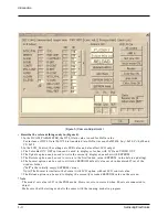
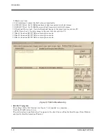
• Describe the relevant things only in (Figure 4).

1. In the DCAM_PARAMETER, the DTL_Glain value is used for HeXa value.

For instance, if DTL_Gain=2631720 is translated into HeXa, it means 0x282828. So y=0x28, Cr=0x28 and
Cb=0x28.

2. In the LCD_Control, the settings are EVR value and also affect LCD output.
3. The Color Bar ON/OFF option can be used to display color bar with LCD and VIDEO OUT.
4. The Update option can be used to write the currently displayed number with EEPROM.
5. The Restore option can be used to restore to the first loaded value (EEPROM  value before updating).
6. The Format option can be used to write the EEPROM default value saved in dscdtuio007.ini. of the

window folder.

("0xff" is the initially empty EEPROM value.)
Note) The Format is similar to the Format with LCD option without LCD control value.

7. The Reload option can be used to display the currently recorded EEPROM value on the screen.

*Note

- The model set value is 007 in the PGM mode. However, error occurred when 80 sets are connected to

adjust.

- Make sure that the testing model is the same with the running model in program.

Samsung Electronics

1-4

Introduction

(Figure 5) Camera Adjustment

I

Содержание SDC-80

Страница 1: ...L SERVICE MANUAL SDC 80 DIGITAL CAMERA SDC 80 SERVICE 1 Introduction 2 Specifications 3 Disassembly and Reassembly 4 Exploded View and Parts List 5 Adjustment 6 Electrical Parts List 7 PCB Diagrams 8 Wiring Diagram 9 Schematic Diagrams Manual DIGITAL CAMERA CONTENTS ...

Страница 2: ...cial servicing information Service Bulletin etc If only parts number changes Just change parts number directly on parts list And if you need more information please see the service bulletin Application Data Page Part Note Cause Solution S Bulletin ...

Страница 3: ...FORMAT DELETE ALL 2 FUNCTION KEY TEST 3 LCD PIXEL TEST 4 LOGO TEST 5 CONTROL LED TEST LCD PANEL TEST 6 MACRO MODE CHECK VIDEO JACK TEST STROBO FLASH JACK CHECK 7 OSD ON SCREEN DISPLAY OFF 8 PC SHOT SELF TIMER SHOT 9 AE ADJUSTMENT 10 3100K 5100K WHITE BALANCE ADJUSTMENT 11 JPEG THUMBNAIL DOWN LOAD 12 BACK FOCUS ADJUSTMENT MODE 13 POWER CONSTANT ON 14 RS 232C CHANGER TEST 15 NTST PAL CONVERT ADJUSTM...

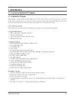
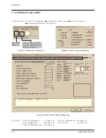
Страница 4: ...ra Power on camera Execute DSCStudio exe in Windows About TAP Camera Adjustment I see Figure 5 Camera Adjustment II see Figure 6 View Graphic File see Figure 7 Test Options see Figure 8 PGM for Manufacturing see Figure 9 Samsung Electronics 1 2 Introduction 1 1 2 DSCStudio Description Start DSC studio Set up Communication port and communication speed see Figure 4 TAP ...

Страница 5: ...estore option can be used to restore to the first loaded value EEPROM value before updating 6 The Format option can be used to write the EEPROM default value saved in dscdtuio007 ini of the window folder 0xff is the initially empty EEPROM value Note The Format is similar to the Format with LCD option without LCD control value 7 The Reload option can be used to display the currently recorded EEPROM...

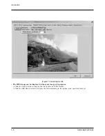
Страница 6: ... image can be displayed without any image edit program 1 Click the Open button to display the file saved as a JPEG format 2 Click the Slid Show button to display the file containing in the option at an specified interval Figure 7 View Graphic File ...

Страница 7: ...media card into PC 16 JPEG Down Load Transfer image in the smart media card into PC 17 Shot 0 Function SHUTTER in camera photo mode 18 Shot 0 Function SHUTTER in camera photo mode 19 Shot 0 Function SHUTTER in camera photo mode Run the PI program The settings of the Test Options see Figure 7 are applied as a sequence Click the START button to run The edit function is enabled when Vs appear in the ...

Страница 8: ...x Height x Width Net Weigh Less than 199g not including battery pack Basic Shooting Mode Full Size Shooting 1152 x 864 SQ HQ General Shooting Standard Shooting VGA Size Shooting 640 x 480 SQ HQ B W Shooting Full Size B W 1152 x 854 SQ HQ Special Shooting Mode Multi Shooting Full Size Division 1152x 864 SQ HQ 4 16 Images Division Continuous Shooting VGA Size continuation 640 x 480 SQ HQ 3 6 Images ...

Страница 9: ...Samsung Electronics 2 2 Specifications MEMO MEMO ...

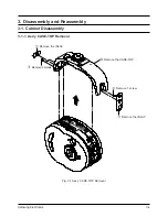
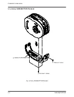
Страница 10: ...ectronics 3 1 3 Disassembly and Reassembly 3 1 Cabinet Disassembly 3 1 1 Ass y CASE TOP Removal Fig 3 1 Ass y CASE TOP Removal Remove the INLAY Remove 2 screws Remove the CASE TOP Remove 1 screw Remove the INLAY ...

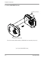
Страница 11: ...Samsung Electronics 3 2 Disassemblr and Reassembly 3 1 2 Ass y CASE BOTTOM Removal Fig 3 2 Ass y CASE BOTTOM Removal Remove the CASE BOTTOM Remove 3 screws Remove 1 screw ...

Страница 12: ...ics 3 4 Disassemblr and Reassembly 3 1 4 Ass y CASE FRONT Removal Fig 3 4 Ass y CASE FRONT Removal Remove 2 screws Remove the CASE FRONT Be careful to assemble MACRO LEVER with LENS MACRO when assembling the case front ...

Страница 13: ...Samsung Electronics 3 6 Disassemblr and Reassembly Fig 3 6 Ass y MAIN Removal 3 1 6 Ass y MAIN Removal Remove the ASSY MAIN Remove the 3screws Remove the FPC MAIN from MAIN PCB ...

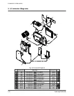
Страница 14: ...ARD MAIN BOARD JACK BOARD MAIN BOARD ASSY LENS MAIN BOARD REAR BOARD MAIN BOARD FUNT BOARD MAIN BOARD TFT LCD FUNT BOARD ASSY STROBO DC BOARD JACK BOARD DC BOARD BATTERY REAR BOARD LCD B L NO NO CONNECTOR CN02 CN02 CN03 CN05 CN04 CNL01 CNF03 CNP02 CNP02 CNB02 CONNECTOR CNP03 CNJ02 LENS FPC CNB01 CNF01 LCD FPC STROBO CNJ03 BATTERY HBL 1 2 3 5 11 13 15 18 9 7 8 ...

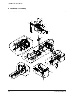
Страница 15: ...Samsung Electronics 4 1 4 1 Cabinet Assembly 4 2 4 2 Parts List 4 3 4 Exploded View and Parts List ...

Страница 16: ...700 106 105 104 103 400 702 402 403 401 703 701 300 302 308 307 306 305 304 303 310 309 702 703 702 702 301 500 702 800 507 702 504 701 701 700 502 503 506 505 701 702 702 501 508 600 601 608 701 610 702 606 705 607 603 602 605 604 609 200 208 207 105 202 203 701 204 702 701 201 205 206 105 ...

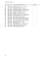
Страница 17: ...8 SDC X80 605 AD99 40009U ASSY MAIN BOARD c SDC X80 ASSY MAIN B 606 AD63 00122A SHIELD SUB PBS T0 15 SDC 80 607 AD97 01702A ASSY SHIELD CASE MAIN SDC 80 608 AD97 00315A ASSY DSC LENS SDC 007 ASSY PANFOCUS 609 AD97 01472A ASSY FPC MAIN SDC 80 FPC MAIN 40 26 T0 6 610 AD41 00097A FFC FUNC 22PIN FLATCABLE 0 3 22 SDC 80 700 6002 001094 SCREW TAPPING CH 0 5 B M1 7 L3 5 NI P 701 AC60 12128B SCREW TAPTITE...

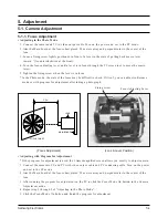
Страница 18: ...ocus may be difficult to check If it isn t you can adjust in Resume mode or with program for adjustment after taking a photograph Adjusting with Program for Adjustment If the program for adjustment is used the 3 times magnified screen allows you exactly to adjust camera 1 Connect the camera to TV and PC with video output cable and PC connecting cable Turn on the power and set to the PC mode 2 Aim ...

Страница 19: ... 1 2 MCLK Adjustment 1 Turn on camera power and set to Photo mode 2 One adjustment point is TP1 MCLK Adjust using CT301 3 Connect probe of frequency counter with TP1 4 Using CT301 adjust it so that MCLK is 54 00MHz 00Hz External view of PCB Main Board component side ...

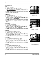
Страница 20: ...e number buttons so that the C level between black and white is 3 0 0 1Vp p 3 Using the UPDATE button store the adjusted value in the EEPROM 4 R BRIGHT 1 TP3 VR R BRT mode Bright wave form 2 Connect the probe of oscilloscope to TP3 VR Press the UP DOWN button or the number buttons so that the B level between pedestals is 3 5 0 1Vp p 3 Using the UPDATE button store the adjusted value in the EEPROM ...

Страница 21: ...Samsung Electronics 5 6 Adjustment MEMO MEMO ...

Страница 22: ...0 2203 000189 C CERAMIC CHIP 100nF 80 20 25V Y5V TP C12 2203 000189 C CERAMIC CHIP 100nF 80 20 25V Y5V TP Loc No Part No Desc Spec Remark C15 2203 000998 C CERAMIC CHIP 0 047nF 5 50V NP0 TP 160 C16 2203 000626 C CERAMIC CHIP 0 022nF 5 50V NP0 TP 160 C17 2203 000189 C CERAMIC CHIP 100nF 80 20 25V Y5V TP C18 2404 000151 C TA CHIP 1uF 20 16V TP 3216 C19 2203 000189 C CERAMIC CHIP 100nF 80 20 25V Y5V ...

Страница 23: ...0V TP 3528 CD35 2203 000189 C CERAMIC CHIP 100nF 80 20 25V Y5V TP CD36 2203 000189 C CERAMIC CHIP 100nF 80 20 25V Y5V TP Loc No Part No Desc Spec Remark CD37 2203 000189 C CERAMIC CHIP 100nF 80 20 25V Y5V TP CD38 2203 000491 C CERAMIC CHIP 2 2nF 10 50V X7R TP 1608 CD39 2203 000189 C CERAMIC CHIP 100nF 80 20 25V Y5V TP CD40 2404 000156 C TA CHIP 1uF 20 35V TP 3528 1 4mm CD42 2203 000189 C CERAMIC C...

Страница 24: ...270ohm 5 1 16W DA TP 1608 R06 2007 000109 R CHIP 1Mohm 5 1 16W DA TP 1608 R07 2007 000074 R CHIP 100ohm 5 1 16W DA TP 1608 R08 2007 000072 R CHIP 47ohm 5 1 16W DA TP 1608 Loc No Part No Desc Spec Remark R09 2007 000084 R CHIP 4 7Kohm 5 1 16W DA TP 1608 R10 2007 000134 R CHIP 33Kohm 5 1 16W DA TP 1608 R11 2007 000134 R CHIP 33Kohm 5 1 16W DA TP 1608 R13 2007 000078 R CHIP 1Kohm 5 1 16W DA TP 1608 R...

Страница 25: ...P 390ohm 5 1 16W DA TP 1608 RL74 2007 000082 R CHIP 3 3Kohm 5 1 16W DA TP 1608 Loc No Part No Desc Spec Remark RL75 2007 000450 R CHIP 180ohm 5 1 16W DA TP 1608 RL81 2007 000125 R CHIP 3 9Kohm 5 1 16W DA TP 1608 RL82 2007 000124 R CHIP 2 2Kohm 5 1 16W DA TP 1608 RL83 2007 000130 R CHIP 39Kohm 5 1 16W DA TP 1608 RL84 2007 000084 R CHIP 4 7Kohm 5 1 16W DA TP 1608 RL85 2007 000102 R CHIP 100Kohm 5 1 ...

Страница 26: ...DP04 0401 001054 DIODE SWITCHING KDS160 85V 300mA SOD 323 DP05 0401 001054 DIODE SWITCHING KDS160 85V 300mA SOD 323 Loc No Part No Desc Spec Remark DP06 0401 001054 DIODE SWITCHING KDS160 85V 300mA SOD 323 DP22 0401 001054 DIODE SWITCHING KDS160 85V 300mA SOD 323 DP23 0401 001054 DIODE SWITCHING KDS160 85V 300mA SOD 323 ICC01 1203 001840 IC BATTERY 3801 SOP 16P 150MIL PLASTIC ICP01 1203 001844 IC ...

Страница 27: ...50ACB 322513 T BJ02 3301 001051 CORE FERRITE BEAD AC 1 6X0 8X0 8mm BJ03 3301 001051 CORE FERRITE BEAD AC 1 6X0 8X0 8mm CJ01 2404 000304 C TA CHIP 22uF 20 6 3V TP 3528 CNJ02 3708 001236 CONNECTOR FPC FC PIC 10P 0 5mm SMD A SN CNJ03 3711 000456 CONNECTOR HEADER 3WALL 4P 1R 1 25mm SMD DJ01 0401 001054 DIODE SWITCHING KDS160 85V 300mA SOD 323 DJ02 0401 001054 DIODE SWITCHING KDS160 85V 300mA SOD 323 D...

Страница 28: ...Samsung Electronics 7 1 7 PCB Diagrams 7 1 Main PCB Rev 02 7 2 7 2 Main PCB Rev 03 7 4 7 3 B L PCB 7 6 7 4 DC PCB 7 8 7 5 Function PCB 7 10 7 6 Jack PCB 7 11 Main PCB ...

Страница 29: ...Samsung Electronics 7 2 PCB Diagrams 7 1 Main PCB Rev 02 C C C Co o o on n n nd d d du u u uc c c ct t t to o o or r r r S S S Si i i id d d de e e e ...

Страница 30: ...Samsung Electronics 7 4 PCB Diagrams 7 2 Main PCB Rev 03 C C C Co o o on n n nd d d du u u uc c c ct t t to o o or r r r S S S Si i i id d d de e e e ...

Страница 31: ...Samsung Electronics 7 6 PCB Diagrams 7 3 B L PCB C C C Co o o on n n nd d d du u u uc c c ct t t to o o or r r r S S S Si i i id d d de e e e ...

Страница 32: ...Samsung Electronics 7 8 PCB Diagrams 7 4 DC PCB C C C Co o o on n n nd d d du u u uc c c ct t t to o o or r r r S S S Si i i id d d de e e e ...

Страница 33: ...ploded View and Parts List 7 5 Function PCB C C C Co o o on n n nd d d du u u uc c c ct t t to o o or r r r S S S Si i i id d d de e e e C C C Co o o om m m mp p p po o o on n n ne e e en n n nt t t t S S S Si i i id d d de e e e ...

Страница 34: ...Samsung Electronics 7 12 PCB Diagrams MEMO MEMO ...

Страница 35: ...Samsung Electronics 8 1 8 Wiring Diagram ...

Страница 36: ...Samsung Electronics 8 2 Wiring Diagram MEMO MEMO ...

Страница 37: ...Diagrams 9 Schematic Diagrams 9 1 CCD Block 9 2 9 2 Drive Block 9 3 9 3 Process Block 9 4 9 4 Function Block 9 5 9 5 LCD Block 9 6 9 6 JACK Block 9 7 9 7 CCD Block 9 8 9 8 Drive Block 9 9 9 9 Process Block 9 10 9 10 Function Block 9 11 ...

Страница 38: ...Samsung Electronics 9 2 Schematic Diagrams 9 2 9 1 Process Block Rev 02 03 Rev 02 Rev 03 ...

Страница 39: ...Samsung Electronics 9 3 Schematic Diagrams 9 2 Drive Block Rev 02 03 ...

Страница 40: ...Samsung Electronics 9 4 Schematic Diagrams 9 3 Mevory Block Rev 02 ...

Страница 41: ...Samsung Electronics 9 5 Schematic Diagrams 9 4 Memory Block Rev 03 ...

Страница 42: ...Samsung Electronics 9 6 Schematic Diagrams 9 5 LCD Block Rev 02 03 ...

Страница 43: ...Samsung Electronics 9 7 Schematic Diagrams 9 6 Back Light Block Rev 02 03 ...

Страница 44: ...Samsung Electronics 9 8 Schematic Diagrams 9 7 DC Block Rev 02 03 ...

Страница 45: ...Samsung Electronics 9 9 Schematic Diagrams 9 8 Charge Block Rev 02 03 ...

Страница 46: ...Samsung Electronics 9 10 Schematic Diagrams 9 9 Function Block Rev 02 03 ...

Страница 47: ...Samsung Electronics 9 11 Schematic Diagrams 9 10 Jack Block Rev 02 03 ...

Отзывы: