


Samsung Electronics
4-37
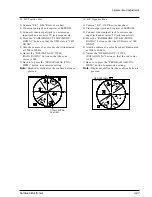
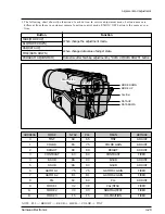
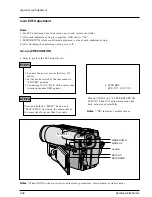
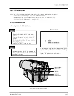
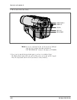
Alignment and Adjustment
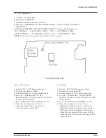
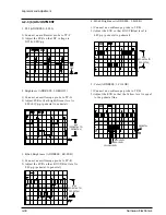
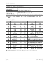
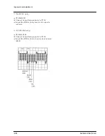
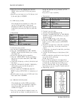
X-TAL
24P-LCD
10P-BL
A
G
B
VCO
VCOM
R
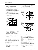
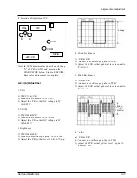
1. VCO
1) TP-VCO & EVR
2) Connect an voltmeter to TP-VCO.
3) Adjust the EVR so that DC voltage is DC
1.6±0.05 V.
2. VCOM
1) TP-COM & EVR
2) Connect an voltmeter to TP-COM.
3) Adjust the EVR so that DC voltage is DC
1.45±0.05 V.
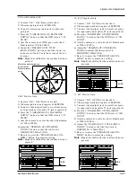
3. Brightness
1) TP-COM & EVR
2) Connect an oscilloscope probe to TP-COM.
3) Adjust the EVR so that level is 6.4± 0.1 Vp-p.
Note: In LCD adjustment mode, when shorting
"A" of PCB to GND and pressing the
START/STOP button. Store in EEPROM.
Reset after adjustment is complete.
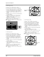
4. R-Sub Brightness
1) TP-R & EVR
2) Connect an oscilloscope probe to TP-R.
3) Adjust the EVR so that pedestal level is equal to
TP-G level.
5. B-Sub Brightness
1) TP-B & EVR
2) Connect an oscilloscope probe to TP-B.
3) Adjust the EVR so that pedestal level is equal to
TP-G level.
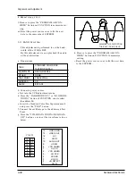
6. Color
a) TP-B & EVR
b) Connect an oscilloscope probe to TP-B.
c) Adjust the EVR so that yellow level is equal to
pedestal level.
LEVEL
(PEDESTAL
TO
PEDESTAL
)
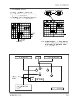
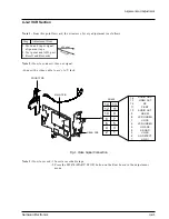
4-2-4 (b) Adjustment
4. Location of Adjustment TP
6.4Vp-p
14P
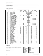
Содержание SCL500
Страница 1: ...SERVICE MANUAL SAMSUNG VPL500 MODEL ...
Страница 7: ...MEMO MEMO Products Specifications and Comparison Chart Samsung Electronics 2 4 ...
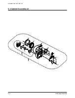
Страница 85: ...Samsung Electronics 5 18 Exploded View and Parts List MEMO MEMO ...
Страница 115: ...7 2 Samsung Electronics PCB Diagrams 7 1 Main PCB Normal Component Side ...
Страница 116: ...7 3 Samsung Electronics PCB Diagrams ...
Страница 117: ...7 4 Samsung Electronics PCB Diagrams 7 2 Main PCB Normal Conductor Side ...
Страница 118: ...7 5 Samsung Electronics PCB Diagrams ...
Страница 119: ...7 6 Samsung Electronics PCB Diagrams 7 3 Main PCB Hi8 Component Side ...
Страница 120: ...7 7 Samsung Electronics PCB Diagrams ...
Страница 121: ...7 8 Samsung Electronics PCB Diagrams 7 4 Main PCB Hi8 Conductor Side ...
Страница 122: ...7 9 Samsung Electronics PCB Diagrams ...
Страница 123: ...7 10 Samsung Electronics PCB Diagrams 7 5 Rear PCB Component Side Conductor Side SCL550 VP L550 Only ...
Страница 124: ...7 11 Samsung Electronics PCB Diagrams 7 6 CCD PCB Component Side Conductor Side ...
Страница 125: ...7 12 Samsung Electronics PCB Diagrams 7 7 CVF PCB Component Side Conductor Side ...
Страница 126: ...7 13 Samsung Electronics PCB Diagrams 7 8 EVF PCB Component Side Conductor Side ...
Страница 127: ...7 14 Samsung Electronics PCB Diagrams 7 9 Function PCB Component Side Conductor Side ...
Страница 128: ...7 15 Samsung Electronics PCB Diagrams 7 10 LCD PCB Component Side Conductor Side ...
Страница 129: ...7 16 Samsung Electronics PCB Diagrams 7 11 Front PCB ...
Страница 130: ...8 1 Samsung Electronics 8 Wiring Diagram ...
Страница 131: ...8 2 Samsung Electronics Wiring Diagram MEMO MEMO ...
Страница 135: ...9 4 Samsung Electronics Schematic Diagrams 9 1 DC DC Converter Main ...
Страница 136: ...9 5 Samsung Electronics Schematic Diagrams 9 2 System Control Servo Main ...
Страница 137: ...9 6 Samsung Electronics Schematic Diagrams 9 3 Video Normal Main ...
Страница 138: ...9 7 Samsung Electronics Schematic Diagrams 9 4 Video Hi8 Main ...
Страница 139: ...9 8 Samsung Electronics Schematic Diagrams 9 5 Audio Main ...
Страница 140: ...9 9 Samsung Electronics Schematic Diagrams 9 6 Camera Main ...
Страница 141: ...9 10 Samsung Electronics Schematic Diagrams 9 7 Rear ...
Страница 142: ...9 11 Samsung Electronics Schematic Diagrams 9 8 CCD ...
Страница 143: ...9 12 Samsung Electronics Schematic Diagrams 9 9 CVF ...
Страница 144: ...9 13 Samsung Electronics Schematic Diagrams 9 10 Front ...
Страница 145: ...9 14 Samsung Electronics Schematic Diagrams 9 11 Function ...
Страница 146: ...9 15 Samsung Electronics Schematic Diagrams 9 12 EVF ...
Страница 147: ...9 16 Samsung Electronics Schematic Diagrams 9 13 LCD ...


