11. High voltage is maintained within specified
limits by close-tolerance, safety-related compo-
nents and adjustments. If the high voltage
exceeds the specified limits, check each of the
special components.
12. Design Alteration Warning :
Never alter or add to the mechanical or elec-
trical design of this unit. Example : Do not
add auxiliary audio or video connectors. Such
alterations might create a safety hazard. Also,
any design changes or additions will void the
manufacturer’s warranty.
13. Hot Chassis Warning :
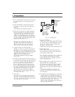
Some TV receiver chassis are electrically
connected directly to one conductor of the AC
power cord. If an isolation transformer is not
used, these units may be safely serviced only
if the AC power plug is inserted so that the
chassis is connected to the ground side of the
AC source.
To confirm that the AC power plug is inserted
correctly, do the following : Using an AC
voltmeter, measure the voltage between the
chassis and a known earth ground. If the read-
ing is greater than 1.0V, remove the AC power
plug, reverse its polarity and reinsert. Re-mea-
sure the voltage between the chassis and
ground.
14. Some TV chassis are designed to operate with
85 volts AC between chassis and ground,
regardless of the AC plug polarity. These units
can be safely serviced only if an isolation trans-
former inserted between the receiver and the
power source.
15. Never defeat any of the B+ voltage interlocks.
Do not apply AC power to the unit (or any of
its assemblies) unless all solid-state heat sinks
are correctly installed.
16. Always connect a test instrument’s ground
lead to the instrument chassis ground before
connecting the positive lead; always remove
the instrument’s ground lead last.
17. Observe the original lead dress, especially near
the following areas : Antenna wiring, sharp
edges, and especially the AC and high voltage
power supplies. Always inspect for pinched,
out-of-place, or frayed wiring. Do not change
the spacing between components and the
printed circuit board. Check the AC power
cord for damage. Make sure that leads and
components do not touch thermally hot parts.
18. Picture Tube Implosion Warning :
The picture tube in this receiver employs
“integral implosion” protection. To ensure
continued implosion protection, make sure
that the replacement picture tube is the same
as the original.
19. Do not remove, install or handle the picture
tube without first putting on shatterproof gog-
gles equipped with side shields. Never handle
the picture tube by its neck. Some “in-line”
picture tubes are equipped with a permanently
attached deflection yoke; do not try to remove
such “permanently attached” yokes from the
picture tube.
20. Product Safety Notice :
Some electrical and mechanical parts have
special safety-related characteristics which
might not be obvious from visual inspection.
These safety features and the protection they
give might be lost if the replacement compo-
nent differs from the original--even if the
replacement is rated for higher voltage,
wattage, etc.
Components that are critical for safety are
indicated in the circuit diagram by shading,
( or ).
Use replacement components that have the
same ratings, especially for flame resistance
and dielectric strength specifications.
A replacement part that does not have the
same safety characteristics as the original
might create shock, fire or other hazards.
Samsung Electronics
1-2
Precautions
Содержание SCD80
Страница 5: ...MEMO MEMO Products Specifications and Comparison Chart Samsung Electronics 2 2 ...
Страница 15: ...Samsung Electronics 3 10 Disassembly and Reassembly MEMO MEMO ...
Страница 43: ...Samsung Electronics 4 28 Alignment and Adjustment MEMO MEMO ...
Страница 45: ...Samsung Electronics 5 2 Exploded View and Parts List 5 1 Ass y CASE REAR ...
Страница 47: ...Samsung Electronics 5 4 Exploded View and Parts List 5 2 Ass y COVER HOUSING 902 903 400 S N A ...
Страница 57: ...Samsung Electronics 5 14 Exploded View and Parts List 5 7 Ass y LCD 580 581 ...
Страница 59: ...Samsung Electronics 5 16 Exploded View and Parts List 5 8 Ass y CAMERA 152 ...
Страница 61: ...Samsung Electronics 5 18 Exploded View and Parts List 5 9 Ass y CVF 519 ...
Страница 63: ...Samsung Electronics 5 20 Exploded View and Parts List 5 10 Ass y EVF ...
Страница 69: ...Samsung Electronics 5 26 Exploded View and Parts List MEMO MEMO ...
Страница 87: ...MEMO MEMO Samsung Electronics 6 18 Electrical Parts List ...
Страница 89: ...7 2 Samsung Electronics PCB Diagrams 7 1 MAIN PCB Component Side ...
Страница 90: ...7 3 Samsung Electronics PCB Diagrams Conductor Side ...
Страница 91: ...7 4 Samsung Electronics PCB Diagrams 7 2 CVF PCB Component Side Conductor Side ...
Страница 92: ...7 5 Samsung Electronics PCB Diagrams 7 3 CCD PCB Component Side Conductor Side ...
Страница 93: ...7 6 Samsung Electronics PCB Diagrams 7 4 JACK PCB Component Side Conductor Side ...
Страница 94: ...7 7 Samsung Electronics PCB Diagrams 7 5 TOP PCB Component Side Conductor Side ...
Страница 95: ...7 8 Samsung Electronics PCB Diagrams 7 6 FUNCTION PCB ...
Страница 96: ...7 9 Samsung Electronics PCB Diagrams 7 7 PVI LCD PCB ...
Страница 97: ...7 10 Samsung Electronics PCB Diagrams 7 8 Sony LCD PCB Component Side Conductor Side ...
Страница 98: ...7 11 Samsung Electronics PCB Diagrams 7 9 EVF PCB Component Side Conductor Side ...
Страница 99: ...7 12 Samsung Electronics PCB Diagrams 7 10 REAR PCB Component Side Conductor Side ...
Страница 100: ...7 13 Samsung Electronics PCB Diagrams 7 11 LEFT PCB Component Side Conductor Side ...
Страница 101: ...7 14 Samsung Electronics PCB Diagrams 7 12 Memory Stick PCB Component Side Conductor Side ...
Страница 103: ...8 2 Samsung Electronics Wiring Diagram MEMO MEMO ...
Страница 105: ...9 2 Samsung Electronics Schematic Diagrams 9 1 System Control ...
Страница 106: ...9 3 Samsung Electronics Schematic Diagrams 9 2 Servo ...
Страница 107: ...9 4 Samsung Electronics Schematic Diagrams 9 3 Timer ...
Страница 108: ...9 5 Samsung Electronics Schematic Diagrams 9 4 Camera ...
Страница 109: ...9 6 Samsung Electronics Schematic Diagrams 9 5 DC DC Converter ...
Страница 110: ...9 7 Samsung Electronics Schematic Diagrams 9 6 Audio ...
Страница 111: ...9 8 Samsung Electronics Schematic Diagrams 9 7 Video ...
Страница 112: ...9 9 Samsung Electronics Schematic Diagrams 9 8 USB ...
Страница 113: ...9 10 Samsung Electronics Schematic Diagrams 9 9 CVF ...
Страница 114: ...9 11 Samsung Electronics Schematic Diagrams 9 10 EVF ...
Страница 115: ...9 12 Samsung Electronics Schematic Diagrams 9 11 PVI LCD ...
Страница 116: ...9 13 Samsung Electronics Schematic Diagrams 9 12 Sony LCD ...
Страница 117: ...9 14 Samsung Electronics Schematic Diagrams 9 13 CCD ...
Страница 118: ...9 15 Samsung Electronics Schematic Diagrams 9 14 TOP BLOCK SCHEMATIC ...
Страница 119: ...9 16 Samsung Electronics Schematic Diagrams 9 15 FUNCTION BLOCK SCHEMATIC ...
Страница 120: ...9 17 Samsung Electronics Schematic Diagrams 9 16 JACK ...
Страница 121: ...9 18 Samsung Electronics Schematic Diagrams 9 17 REAR ...
Страница 122: ...9 19 Samsung Electronics Schematic Diagrams 9 18 LEFT ...
Страница 123: ...9 20 Samsung Electronics Schematic Diagrams 9 19 Memory Stick 1 ...
Страница 124: ...9 21 Samsung Electronics Schematic Diagrams 9 20 Memory Stick 2 ...
Страница 125: ...MEMO MEMO 9 22 Samsung Electronics Schematic Diagrams ...
Страница 127: ...Ⓒ Samsung Electronics Co Ltd APR 2001 Printed in korea AD68 30200A ELECTRONICS 표지 영문 2001 7 4 2 0 PM 페이지2 ...
Страница 157: ...1 30 Samsung Electronics MEMO 1 동작 영문 2001 7 4 2 4 PM 페이지1 30 ...


