background image

Disassembly & Reassembly

Samsung Electronics

3-5

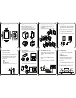
3-1-11 Separation of ASSY PDP MODULE P-X MAIN BOARD

Part Name

Description

Description Photo

Flat Cable

Detach all Connectors from the X Main Board.

To separate the Flat Cable of the X-Board, press the 

upper and the lower sides of the connector.

: Pinch the sides, but then push down in the ribbon, it 

should slide out after that. 

X-Main

Board

Remove 6 screws.

: PH,+,WWP,M3,L8,NI PLT

Remove the X-Main Board

.

Содержание PN42A450P1D

Страница 1: ...embly Reassembly 4 Troubleshooting 5 Exploded View Part List 6 Wiring Diagram 7 Schematic Diagram SERVICE Manual PN42A450P1D PLASMA DISPLAY TV Chassis F45A N_HD _Pyrope Model PN42A450P1DXZC Refer to the service manual in the GSPN see the rear cover for the more information ...

Страница 2: ...stic law Samsung Electronics Co Ltd Mar 2008 Printed in Korea AA82 05103A Area Web Site North America service samsungportal com Latin America latin samsungportal com CIS cis samsungportal com Europe europe samsungportal com China china samsungportal com Asia asia samsungportal com Mideast Africa mea samsungportal com GSPN Global Service Partner Network ...

Страница 3: ...ifications Analysis 2 3 2 3 Accessories 2 4 Chapter 3 Disassembly Reassembly 3 1 Overall Disassembly Reassembly 3 1 Chapter 4 Troubleshooting 4 1 Troubleshooting 4 1 4 2 Adjustment 4 16 4 3 Upgrade 4 32 Chapter 5 Exploded View Part List 5 1 PN42A450P1DXZC Exploded View 5 1 5 2 PN42A450P1DXZC Service Item 5 3 Chapter 6 Wiring Diagram 6 1 Overall Wiring 6 1 Chapter 7 Schematic Diagram 7 1 Circuit De...

Страница 4: ... insulated transformers the product can only be repaired safely when the chassis is connected to the earth end of the AC power source To make sure the AC power cord is properly connected follow the instructions below Use the voltmeter to measure the voltage between the chassis and the earth ground If the measurement is over 1 0V unplug the AC power cord and change the polarity before re inserting ...

Страница 5: ...eplaced with another irregular one the safety or protective features will be lost even if the new one has a higher voltage or more watts Critical safety parts should be bracketed with Use only regular parts for replacements in particular flame resistance and dielectric strength specifications Irregular parts or materials may cause electric shock or fire Precaution 1 2 Samsung Electronics ...

Страница 6: ...istance between the blade of the AC plug and that of the conductive material should be more than 1 7 Any B interlock should not be damaged If the metal heat sink is not properly installed no connection to the AC power should be made 8 Make sure the grounding lead of the tester is connected to the chassis ground before connecting to the positive lead The ground lead of the tester should be removed ...

Страница 7: ...ns for soldering purposes 6 Use only anti static solder removal devices Most solder removal devices do not support an anti static feature A solder removal device without an anti static feature can store enough static electricity to cause damage to the ESD 7 Do not remove the ESD from the protective box until the replacement is ready Most ESD replacements are covered with lead which will cause a sh...

Страница 8: ...ositioning the product Also check the antenna cable or the external connectors if they are fully unplugged Damage to the cord may cause fire or electric shock 6 Keep the antenna far away from any high voltage cables and install it firmly Contact with the high voltage cable or the antenna falling over may cause fire or electric shock 7 When connecting the RF antenna check for a DTV receiving system...

Страница 9: ...1 6 Samsung Electronics MEMO ...

Страница 10: ...2 4 inches with stand 48 4 x 29 8 x 3 7 inches without stand 48 4 x 32 0 x 12 4 inches with stand Weight 59 31 lbs without stand 67 24 lbs with stand 75 41 lbs without stand 81 57 lbs with stand PC Resolution 1024 x 768 75Hz 1360 x 768 60Hz Power consumption 330W 470W Voltage AC 100 240V 60Hz ANTENNA input ANT AIR IN or CABLE IN 75Ω unbalanced VIDEO input AV1 AV2 S VIDEO1 COMPONENT1 480i 480p 720p...

Страница 11: ... can listen to 5 1 channel sound through the home theater s speakers Otherwise you can only listen to 2 channel stereo sound in other cases Make sure to connect the Digital Audio IN Optical of the home theater and the TV correctly to listen to TV sound through the home theater However you cannot listen to sound from the BD recorder that is sent to the home theater via the TV in 5 1 channel sound b...

Страница 12: ...icture Brightness 1 500 Cd m2 1 300 Cd m2 1 500 Cd m2 Contrast Ratio 10000 1 10000 1 10000 1 Picture Enhacer FBE3 FBE3 FBE2 Comb Filter Audio Equalizer 5 Band 5 Band 5 Band Auto Volume Control Surround Sound SRS TruSurround XT SRS TruSurround XT SRS TruSurround XT Speaker Output 10W 10W 10W 10W 10W 10W Features PIP X X Double Window X X Caption Still Image X X EPG My Color Control Energy Saving An...

Страница 13: ...8 01399B Warranty Card Registration Card Safety Guide Manual AA68 03242L Cloth Clean BN63 01798A Ferrite Core for Power Cord 3301 001305 Cover Bottom Screws 2ea BN63 03055A 6003 001621 Accessories that can be purchased additionally S VIDEO Cable 47 244 inches BN39 00149A Electronics Store Internal shopping mall HDMI Cable 118 11 inches BN39 00641A HDMI DVI cable 118 11 inches BN39 00643A Component...

Страница 14: ...ssories Item Item code Remark Accessories that can be purchased additionally Optical Cable None Electronics Store Internal shopping mall PC Cable 72 047 inches BN39 00115A PC Audio Cable 78 740 inches BN39 00061B Antenna Cable 118 11 inches BN39 00333A ...

Страница 15: ...2 6 Samsung Electronics MEMO ...

Страница 16: ...P REAR Notice Be sure to separate the power cord before disassembling the unit Discharge the capacitors first when separating PCB s with high capacity capacitors such as SMPS X Main Board Y Main Board etc A spark may be generated by the electric charge and there is danger of electronic shock Check that the cables are properly connected referring to the circuit diagram when disassembling or assembl...

Страница 17: ... L10 ZPC BLK Separate FILTER EMI AC LINE from bracket 3 1 4 Separation of BRACKET PCB Part Name Description Description Photo Bracket PCB Remove 2 screw BH B M4 L3 ZPC BLK Remove 2 screw BH S M4 L10 ZPC BLK Remove the BRACKET PCB 3 1 2 Separation of ASSY PCB MISC MAIN Part Name Description Description Photo Main Board Detach all connectors from the Main Board Remove 4 screws PH WWP M3 L8 NI PLT Re...

Страница 18: ...ove Wall Bracket Please lay the PDP panel face down on a soft surface when separating front cover 3 1 5 Separation of ASSY BRACKET 42 Part Name Description Description Photo Bracket Remove 2 screws BH PT S Tite M4 L10 ZPC BLK Remove 2 screws BH B M4 L3 ZPC BLK Remove Bracket 3 1 6 Separation of ASSY BRACKET 50 Part Name Description Description Photo Bracket Remove 2 screws BH PT S Tite M4 L10 ZPC ...

Страница 19: ...scription Photo SMPS Detach all connectors from the SMPS Remove 8 screws PH WWP M3 L8 NI PLT Remove the SMPS Wear gloves when handling the power board as there may be some remaining electrical charge in the capacitor Specifically avoid touching any part of the capacitor 3 1 8 Separation of ASSY SPEAKER P Part Name Description Description Photo Speaker Disconnect left speaker cable from right speak...

Страница 20: ... Description Photo Flat Cable Detach all Connectors from the X Main Board To separate the Flat Cable of the X Board press the upper and the lower sides of the connector Pinch the sides but then push down in the ribbon it should slide out after that X Main Board Remove 6 screws PH WWP M3 L8 NI PLT Remove the X Main Board ...

Страница 21: ...e Description Description Photo Flat Cable Detach the 6 scan board connectors from the panel 42 Y Scan Board Remove 3 screws PH WWP M3 L8 NI PLT 50 Y Scan Board Remove 9 screws PH WWP M3 L8 NI PLT Y Scan Board Remove 4 screws PH WWP M3 L8 NI PLT Detach all connectors from the Y Main Board This is only for 42 ...

Страница 22: ...l bar you should lift up the panel a little 50 Still Bar Remove 3 screws PH WWP M3 L8 NI PLT Remove the still bar Before removing the still bar you should lift up the panel a little 42 Buffer Board Detach the all connectors from the buffer board Remove 6 screws PH WWP M3 L8 NI PLT Remove the E Board and F Board 50 Buffer Board Detach the all connectors from the buffer board Remove 7 screws PH WWP ...

Страница 23: ... PCB FUNCTION DECO LED Part Name Description Description Photo Function Board Remove 3 screws BH B M4 L3 ZPC BLK 3 1 14 Separation of ASSY PANEL BRACKETS Part Name Description Description Photo Panel Brackets Remove 7 screws BH B M4 L3 ZPC BLK Remove the Side Panel Brackets ...

Страница 24: ... or damaged cable Check to see if there is a disconnected or loose cable connection Check to see if the cables are connected according to the connection diagram 2 Check the power input to the Main Board 3 Check the voltage in and out between the SMPS Main Board between the SMPS X Y Main Board and between the Logic Boards 4 Troubleshooting 4 1 Troubleshooting ...

Страница 25: ...ted or the Main Board or SMPS is not functioning In this case check the following Check the internal cable connection status inside the unit Check the fuses of each part Check the output voltage of SMPS Replace the Main Board Troubleshooting Procedures Is the AC IN socket connector and the SMPS CN800S connected Insert the AC in connector and the SMPS CN800S connector Is the Fuse F801S of the SMPS ...

Страница 26: ...mblies by connecting the cables one by one Troubleshooting Procedures Caution When separating and connecting the cables such as CN810 CN809 CN808 CN807 of the Main SMPS CN4701 of the X Main Board and CN5707 of the Y Main Board a spark may be generated by the electric charge of the high capacity capacitor Therefore wait some time after disconnecting the power cord from the unit Does the symptom con...

Страница 27: ...ing and connecting the cables such as CN810 CN809 CN807 of the Main SMPS CN4701 of the X Main Board and CN5707 of the Y Main Board a spark may be generated by the electric charge of the high capacity capacitor Therefore wait some time after disconnecting the power cord from the unit CN810 CN809 CN807 Are the Vs and Va voltages normal after removing all cables from the SMPS CN810 CN809 CN807 Replac...

Страница 28: ... is not functioning Speaker defect Troubleshooting Procedures Is the cable connection between the Main Board and the speaker properly connected Connect the cable properly or replace the cable if necessary Is the output voltage of SMPS normal CN801 13 Replace the SMPS Replace the Main Board Is the speaker output terminal of the Main Board normal Replace the Speaker Yes No No No Yes Yes 42 50 is alm...

Страница 29: ...is OK Major Checklist Check the antenna connection settings Air NTSC ATSC Cable NTSC Check the CVBS cable connection Check the power input of the Main board Troubleshooting Procedures Is the antenna connection setting properly configured Configure properly Replace the SMPS Check CN1001 pin2 for 5V Replace the Main Board No No Yes Yes ...

Страница 30: ... 4 7 STBY Normal Abnormal Check the UB801 DX807 Multi Normal Abnormal Check the UB801 DX806 DX809 VS VA Check the U804 DS823 DS824 DS825 Abnormal Check the Other board Image Board or Driver Board or Cable Power ON ྛ SMPS Troubleshooting ...

Страница 31: ...l Image not open or short is no screen Y MAIN X MAIN Logic Main Sustain Open Some horizontal lines don t exist on screen Scan Buffer FPC of X Y Sustain Short Some horizontal lines appear to be linked on screen Scan Buffer FPC of X Y Address Open Some vertical lines don t exist on screen Logic Main Logic Buffer TCP Address Short Some vertical lines appear to be linked on screen Logic Main Logic Buf...

Страница 32: ...k the input voltage YES NO YES NO Y MAIN Check several points FUSE FET DIODE Y MAIN Normal State Replace the Board Replace the Board OK OPEN SHORT OK F5000 for VDD F5801 for Vs F5800 for VCC Q5500 Q5200 Q5201 Q5202 Q5203 Q5400 Q5401 Q5402 Q5300 D5105 D5104 D5103 Q5101 D5101 Q5100 X MAIN Check several points FUSE FET DIODE X MAIN Normal State Replace the Board Replace the Board OK OPEN SHORT OK F40...

Страница 33: ...RT OK F5000 for VDD F5801 for Vs F5800 for VCC Q5500 Q5200 Q5201 Q5202 Q5203 Q5400 Q5401 Q5402 Q5300 Q5101 Q5100 X MAIN Check several points FUSE FET X MAIN Normal State Replace the Board Replace the Board OK OPEN SHORT OK F4001 for VCC F4003 for Vs F4005 for VDD F4004 for Ve Q4002 Q4202 Q4004 Q4003 Q4101 Q4001 Q4007 Q4006 Q4005 Abnormal Display Abnormal Image is on Screen except abnormality in Su...

Страница 34: ...echeck the status Done Defect is from Y buffer Replace the Panel There is a defect on the FPC OK NG Sustain Short some horizontal lines appear to be linked on Video Y FPC Sustain Short Discharging in unwanted Scan line After Changing Y buffer recheck the status Done Defect is from Y buffer OK NG Replace the Panel There is a defect on the FPC ...

Страница 35: ...nternal mode screen is normal Reload the data onto the MICOM and recheck it Check if there is an open or short circuit on the Buffer Board and the Logic Main address data output section Check the FFC connection status Check the detailed waveform and control the signal waveform OK NG OK NG Check if a specific TCP Block screen is displayed abnormally OK NG OK Replace Logic Main Address Buffer E or F...

Страница 36: ... upper lower buffers E F COF defect burnt Replace the module A green screen appears when the TV is turned on The Scale is not reseting Replace the Main board The OSD box appears but there is no text Incorrect program version Check the version of each program Replace the Main board A blank upper or lower block appears on the screen Upper Lower Y Buffer defect Replace the corresponding upper lower b...

Страница 37: ...icture does not appear Replace the Main board A vertical green line appears on the screen The SMPS voltage is incorrect Adjust the SMPS voltage according to the voltage printed on the module label Dim screen blurred in red X Main board defect Replace the X Main board A blank screen appears Replace the Y Main board ...

Страница 38: ...ODULE P LOGIC MAIN Blank screen Screen noise 5 ASSY PDP MODULE P Y MAIN SCAN BUFFER Row Bar screen is blank 42 Only 6 ASSY PDP MODULE P ADDRESS E BUFFER Corresponding Buffer Board block screen is blank 7 ASSY PDP MODULE P ADDRESS F BUFFER Corresponding Buffer Board block screen is blank 8 ASSY PCB MISC MAIN No Power Abnormal screen for each input source PIP screen trouble Sound trouble 9 ASSY BOAR...

Страница 39: ...eplacement of Board If adjustment equipment is available PDP Option of Factory Mode set the Factory Data Type item as the suitable value of relevant model Adjust Calibration of Factory Mode for each mode Adjust White Balance of Factory Mode If adjustment equipment is not available Write down the value of HDMI White Balance of Factory Mode before replacing Board PDP Option of Factory Mode set the F...

Страница 40: ... Using the SOURCE key you can switch AV modes 5 Initial SERVICE MODE DISPLAY State The version of the firmware displayed at the bottom of the screen may differ and the firmware is subject to change for the improvement of product functions If you have adjusted the settings in Service Mode you have to reset the product If you exit Service Mode without reset DNIe vlaue keeps Off regardless of setting...

Страница 41: ...libration PC Calibration HDMI Calibration 2 ADC Target Item Default data 1st_AV_Low 18 1st_AV_High 220 1st_AV_Delta 1 1st_COMP_Low 16 1st_COMP_High 235 1st_COMP_Delta 1 1st_PC_Low 1 1st_PC_High 235 1st_PC_Delta 1 2nd_AV_Low 1 2nd_AV_High 235 2nd_AV_Delta 1 2nd_COMP_Low 1 2nd_COMP_High 235 2nd_COMP_Delta 1 2nd_PC_Low 1 2nd_PC_High 235 2nd_PC_Delta 1 2nd_HDMI_Low 1 2nd_HDMI_High 235 2nd_HDMI_Delta 1...

Страница 42: ...6 110 110 112 2nd_G offset 128 108 113 110 112 2nd_B offset 128 106 111 110 112 2nd_R gain 128 128 118 128 118 2nd_G gain 128 128 117 128 118 2nd_B gain 128 1150 118 128 118 Item Default data LCD PDP LCD Model Select L450 Inch 32 Inch Panel Option 32AM Dimming INT Mirror OFF AV Number 2 COMP Number 2 HDMI Number 3 Light Effect ON HeadPhone ON Anynet HDMI CEC ON Carrier Mute OFF Volume Curve Large ...

Страница 43: ...Out Format Vesa FBE In Format Vesa FBE Out Format Vesa Hotel Option EDID HDCP Key Download Item Default data TV AV S_Video Component PC DTV HDMI Remark Sub Brightness 128 128 128 128 128 R Offset 128 128 128 128 128 G Offset 128 128 128 128 128 B Offset 128 128 128 128 128 Sub Contrast 128 128 128 128 128 R Gain 128 128 128 128 128 G Gain 128 128 128 128 128 B Gain 128 128 128 128 128 ...

Страница 44: ...W1_Rgain W1_Bgain W1_Roffset W1_Boffset NOR_Rgain NOR_Bgain NOR_Roffset NOR_Boffset C2_Rgain C2_Bgain C2_Roffset C2_Boffset Movie Contrast Movie Bright Movie Color Movie Sharpness Movie Tint Movie Backlight Movie Gamma 8 EPA Standard Item Default data Standard Contrast 80 Standard Brightness 45 Standard Sharpness 50 Standard Color 50 Standard Tint 0 Standard Backlight 7 ...

Страница 45: ... Mean Offset2 235 235 235 235 235 235 235 235 Mean Slope 112 112 112 112 112 112 112 112 ACR Offset 10 10 10 10 10 10 10 10 ACR Th1 10 10 10 10 10 10 10 10 ACR Th2 110 110 110 110 110 110 110 110 Skin Enable ON ON ON ON ON ON ON ON Skin UV 128 128 128 128 128 128 128 128 Sub color 128 128 128 128 128 128 128 128 M Skin UV 128 128 128 128 128 128 128 128 M Sub color 128 128 128 128 128 128 128 128 ...

Страница 46: ...H2 Gain 0x08 0x08 0x08 0x08 0x08 0x08 0x08 0x08 0x08 0x08 H3 Gain 0x08 0x08 0x08 0x08 0x08 0x08 0x08 0x08 0x08 0x08 H4 Gain 0x08 0x08 0x08 0x08 0x08 0x08 0x08 0x08 0x08 0x08 V1 Gain 0x28 0x28 0x28 0x28 0x28 0x28 0x28 0x28 0x28 0x28 V2 Gain 0x08 0x08 0x08 0x08 0x08 0x08 0x08 0x08 0x08 0x08 H overshoot 0xFF 0xFF 0xFF 0xFF 0xFF 0xFF 0xFF 0xFF 0xFF 0xFF V overshoot 0x60 0x60 0x60 0x60 0x60 0x60 0x60 0...

Страница 47: ...Option Item Default data control register Range Remark Pixel Shift Test Off ON OFF Panel Pattern Select 0 Panel Resolution Panel Inch Panel Version Panel Temperature Logic SW Version Model Select P450 Factory Data Type 42SP5 Checksum MB SW Off MB Offset 0xC0 Ve Signal Control 0xBFFF FRC Mode 100Hz FRC DBG MarkOn 0 17 Checksum 18 Reset ...

Страница 48: ...n 24 Chess Pattern 4 Use Equipment CA210 Master MSPG925 Generator Use other equipment only after comparing the result with that of the Master equipment Chess Pattern Input mode Calibration Pattern CVBS IN Model_ 1 Perform in NTSC B W Pattern 24 Lattice Component IN Model_ 6 Perform in 720p B W Pattern 24 Lattice PC Analog IN Model_ 21 Perform in VESA XGA 1024x768 B W Pattern 24 Lattice HDMI IN Per...

Страница 49: ... is complete it returns to the high level menu 8 You can see the change of the Comp Calibration status from Failure to Success Method of Color Calibration PC 1 Apply the VESA XGA Lattice N0 21 pattern signal to the PC IN port 2 Press the Source key to switch to PC mode 3 Enter Service mode 4 Select the Calibration menu 5 Select the PC Calibration menu 6 In PC Calibration Off status press the key t...

Страница 50: ...ut to HDMI mode Enter the White Balance menu of service mode Contact CA 210 sensor to glass filter Adjust the low light Adjust Sub Bright LBE to set the Y value Adjust R Offset x and B Offset y to the color coordinates Do not adjust G Offset data Adjust the high light Adjust Sub Contrast LBE to set the Y value Adjust R Gain x and B Gain y to the color coordinates Do not adjust the G gain data SAMS...

Страница 51: ...mode CA 210 x Y L T K MPCD CVBS NTSC H L 278 FIX 10 500 0 Sub_CT 128 L L 278 10 5 cd 11 000 3 3 0 Ft COMP 720P H L 278 FIX 10 500 0 Sub_CT 128 L L 278 10 3 cd 11 000 6 3 0 Ft HDMI 720P H L 278 FIX 10 500 0 Sub_CT 128 L L 278 10 3 cd 10 500 0 3 0 Ft ...

Страница 52: ...items listed after changing each Replaced assembly items Check Items ASSY PCB MISC MAIN 1 Auto Program 2 White Balance Adjust SMPS PDP TV Vs Va voltage check and adjust ASSY PDP MODULE P LOGIC MAIN Not to be adjusted ASSY PDP MODULE P X MAIN ASSY PDP MODULE P Y MAIN ASSY PDP MODULE P Y MAIN SCAN BUFFER ASSY PDP MODULE P Y MAIN SCAN BUFFER ASSY PDP MODULE P ADDRESS E BUFFER ASSY PDP MODULE P ADDRES...

Страница 53: ...IN voltage Vs Va Value Board Adjustment Vs 210 SMPS Va 55 Vset Ve 95 Vscan 190 Voltage Adjustment 1 After replacing the SMPS or PDP panel you must adjust the voltage referring to the voltage label printed on the panel If you do not adjust the voltage an abnormal discharge symptom may appear ...

Страница 54: ...s Test Point Set the main reset rising 60usec falling 80usec by change the value of variable resistor 42 50 Test Point The picture is only for 50 42 has only Falling ramp variable resistor 60usec 80usec Rising ramp variable resistor Falling ramp variable resistor ...

Страница 55: ...Upgrade in Menu SETUP Select the SW Upgrade from the menu Select USB from the menu The banner OSD Scaning for USB is displayed The banner OSD Upgrade version to version is displayed Select Yes The banner OSD Upgrade version to version is displayed It takes about 30 sec Warning Don t remove USB flash driver during upgrade The banner OSD Upgrade is completed is displayed when the upgrade is complete...

Страница 56: ...ecking in the User Menu Select the Setup menu in the Menu screen Place the cursor over the SW Upgrade of Setup and press the info key on the remote control The version of the program is displayed at the bottom of the Menu screen 2 How to check Program Version on factory mode PROGRAM VERSION PROGRAM VERSION ...

Страница 57: ...s 5 1 Exploded View Part List 5 Exploded View Part List 5 1 PN42A450P1DXZC Exploded View T0003 M0112 M0150 M0102 T0603 T0056 M0145 M0150 M0146 M0149 T0456 M0027 M0523 T0044 T0165 M0412 M0013 T0079 M0125 M0523 T0175 T0175 ...

Страница 58: ...T P FILTER BOTTOM P450 42Inch 1 S N A M0150 BN96 06748A ASSY BRACKET P SUPPORT FILTER P410 42Inc 1 S N A M0412 BN96 06697D ASSY BRACKET P PCB 42P450 SEA SECC T0 5 1 S N A M0523 BN96 06753A ASSY BRACKET P SUPPORT STAND P410 42Inch 1 S N A M0523 BN96 06756A ASSY BRACKET P WALL P410 42Inch SECC T1 2 S A T0003 BN96 06769A ASSY COVER P FRONT P450 42Inch ABS PMMA 1 S A T0044 BN96 07188A ASSY PDP MODULE ...

Страница 59: ...D W3 1 T0038 BN96 06762A ASSY PDP P ADDRESS E BUFFER PL42AX030A 4 1 T0039 BN96 06763A ASSY PDP P ADDRESS F BUFFER PL42AX030A 4 1 T0044 BN96 07188A ASSY PDP MODULE P S42AX YB04 42HD W3 PL4 1 T0045 BN96 06757A ASSY PDP P X MAIN BOARD PL42AX030A 42HD 1 T0045 BN96 06758A ASSY PDP P X MAIN BUFFER PL42AX030A 42HD 1 T0074 BN59 00687A REMOCON TM 96B 49 AMERICA 1 T0079 BN94 01461A ASSY PCB MISC MAIN PN42A4...

Страница 60: ...1 CN5707 CN807 CN809 CN808 CN810 CN4701 CN4002 CN4001 CN4004 CN2004 CN2600 CN2610 CN2510 CN1 CN3 CN800 LOGIC BOARD SMPS X DRIVE Y DRIVE Y MAIN SCAN AC INLET F BUFFER FUNCTION POWER SW CN2609 CN2000 CN2001 CN2006 SPEAKER CN801 CN2002 CN202P CN201 CN401 MAIN BOARD 8 9 10 11 CN2028 5 6 7 CN101 CN902 2 CN2003 E BUFFER CN2500 CN2509 1 4 42 Overall Wiring ...

Страница 61: ...OWER SW Y MAIN SCAN LOW CN2609 CN2003 CN2000 CN2001 CN2006 CN2005 SPEAKER CN801 CN2002 MAIN BOARD CN2500 CN2509 E BUFFER 6 7 8 10 11 9 2 1 AC INLET CN202P CN201 CN401 CN101 CN902 4 5 50 Overall Wiring The code number of cable Lead connector can be changed see 5 Exploded View Part List Wiring Diagram 6 2 Samsung Electronics Use LVDS POWER CABLE AC INLET Code 42 BN96 07158K 50 BN96 07158F BN39 00827...

Страница 62: ...N101 MAIN B D CN801 MAIN SMPS CN101 MAIN B D CN801 MAIN SMPS Pin No Signal Pin No Signal Pin No Signal Pin No Signal 1 NC 13 5V 1 PS_ON 13 5V 2 SW_POWER 14 5V 2 NC Auto_V 14 5V 3 GND 15 5V 3 STBY 15 5V 4 STD_VCC 16 5V 4 GND_STBY 16 5V 5 GND 17 GND 5 GND_18V AMP 17 GND_12V 6 GND 18 GND 6 GND_18V AMP 18 GND_12V 7 18V 19 GND 7 18V AMP 19 12V 8 18V 20 13V 8 18V AMP 20 GND_12V 9 GND 21 13V 9 GND_5V 21 ...

Страница 63: ... TXC 22 GND 33 GND CN810 SMPS CN5707_42 Y B D CN5407_50 Y B D Pin No Signal 1 Vg 2 GND 3 GND 4 GND 5 Vs 6 Vs CN809 SMPS CN4701 X B D Pin No Signal 1 Vg 2 GND 3 GND 4 Vs 5 Vs CN808 SMPS CN2609 E BUFFER Pin No Signal 1 Va 2 GND 3 5 3V CN401 MAIN B D SPEAKER Pin No Signal 1 R _OUT 2 R _OUT 3 L _OUT 4 L _OUT CN202P MAIN B D FUNCTION Pin No Signal 1 KEY_INPUT1 2 KEY_INPUT2 3 GND CN800 SMPS AC INLET Pin...

Страница 64: ...from AC inlet CN4002 CN4002 Horizontal X scan line of Module and X scan Connect first Block CN4001 CN4001 Horizontal X scan line of Module and X scan Connect second Block CN4000 Horizontal X scan line of Module and X scan Connect third Block CN2000 CN2000 Power input connect 10pin of Logic Board from SMPS CN2001 CN2001 Image signal LVDS connect 41pin of Logic board from Main Board CN2002 CN2002 Y ...

Страница 65: ...6 6 Samsung Electronics MEMO ...

Страница 66: ...d decodes the video signal encoded by the Video Board outputs the ADDRESS data signal for each pattern and generates X and Y drive signals The Address Buffer Board buffers and transfers the ADDRESS data output signal using TCP IC LVDS with built in video signal processing W L error diffusion APC FCR etc applied and 1 ASIC chip Outputs the address Drive IC control and data signals to the Buffer Boa...

Страница 67: ...7 2 Samsung Electronics MEMO ...

Страница 68: ... FGND DMC2_2 5V A5V_1 FGND A5V FGND B13V B5V B5V_TUNER A3 3V_LPLL B13V FGND FGND A5V_1 B13V_S FGND FGND FGND FGND DDR_2 5V A3 3V_SIF A3 3V_AU FGND DMQ1_2 5V FGND DMQ2_2 5V FGND A3 3V_ADC FGND FGND A3 3V FGND FGND FGND A3 3V_VDDP FGND B5V A3 3V_MEMPLL A3 3V FGND FGND FGND A3 3V_MPLL VCC_PANEL A3 3V A5V_1 FGND FGND FGND FGND FGND FGND FGND FGND A5V A5V 100UF 10uF 10V 100nF 16V 100nF 6 3V 1UF 10V 10u...

Страница 69: ...3OHM 33OHM 33OHM MDATA 7 DQS 3 MDATA 31 MDATA 30 MDATA 29 MDATA 28 33OHM 33OHM 33OHM MDATA 26 33OHM MDATA 25 33OHM 33OHM MDATA 16 MDATA 18 MDATA 19 33OHM MDATA 20 MDATA 21 MDATA 23 33OHM 33OHM 33OHM 33OHM MVREF 2 33OHM MDATA 27 MCLK MADR 1 MADR 0 WEZ SMAW200 10P MADR 4 SDA DQS 2 33OHM CKE BA0 MADR 12 MDATA 0 CAS MDATA 31 DQS 0 MCLK DQS 1 DQM 2 DQM 0 MADR 12 BA0 MDATA 12 33OHM CN_S_010 DQM 3 MVREF ...

Страница 70: ... M H O 0 0OHM 0OHM M H O 0 0OHM L E N A P _ L C S M H O 0 M H O 0 M H O 0 M H O 0 M H O 0 M H O 0 8 LV_DIR 8 USB_DP LV_DIR 7 0 1 2 3 4 5 6 7 9 7 909ohm LV_FBE 1 0 1 2 5 0OHM 47ohm 100nF VIDEO2_CVBS 10KOHM 10KOHM 10V 10uF 100nF 16V 1 16W 47ohm 16V 100OHM 100OHM M H O 0 16V 47NF 16V 47NF 47NF 16V 16V 16V 2 2UF 2 2UF 16V 2 2UF 16V 2 2UF 16V 2 2UF 16V 16V 2 2UF 16V 2 2UF 0OHM 0OHM F U 1 F n 0 0 1 V 6 ...

Страница 71: ... I2C_ADDR1 TXCLKOUT TXCLKOUT I2C_ADDR0 Invert_VSYNC Invert_HSYNC FBE_RESET M H O K 7 4 SDA I2C_ADDR1 1 5KOHM PLL_FILTER 1 16W 4 7KOHM W 6 1 1 1 16W 4 7KOHM I2C_ADDR0 SCL BEAD_CHIP BEAD_CHIP BEAD_CHIP BEAD_CHIP 6 8 9 5 3 2 1 0 GND_R_RING GND_R_RING GND_R_RING GND_R_RING GND_R_RING GND_R_RING PWR_R1_RING GND_R_RING PWR_R1_RING PWR_R1_RING PWR_R1_RING GND_R_RING GND_R_RING GND_R_RING AVDD33A_1 AVDD33...

Страница 72: ...V 6 1 F n 0 0 1 M H O M 1 100nF 16V 100nF 16V V 6 1 F n 0 0 1 V 6 1 F n 0 0 1 V 6 1 F n 0 0 1 F n 0 0 1 V 6 1 F n 0 0 1 V 6 1 F n 0 0 1 V 6 1 F n 0 0 1 100nF 16V 100nF 16V 16V 100nF V 6 1 F n 0 0 1 V 6 1 F n 0 0 1 16V 100nF 470OHM 47ohm 47ohm 47ohm 1KOHM M H O K 1 M H O K 1 1KOHM 1KOHM 1KOHM 10V 10uF 10uF 10V 200Kohm W 6 1 1 M H O K 1 100KOHM KTC3875S Y 47NF 25V H U 0 2 2 FGND FGND B3 3V FGND FGND...

Страница 73: ... Z L R V 2 8 10UH 2 8 Z L R V 2 8 2 8 Z L R V 2 8 V 8 4 H T G 0 3 C 3 S D C V 8 4 H T G 0 3 C 3 S D C H T G 0 3 C 3 S D C V 8 4 V 8 4 2 8 Z L R V 2 8 2 8 Z L R V 2 8 V 8 4 10UH 2 8 Z L R V 2 8 V 2 8 2 8 Z L R COMP2_IDENT M_SL_OUT VIDEO1_IDENT CDS3C30GTH 48V H T G 0 3 C 3 S D C H T G 0 3 C 3 S D C H T G 0 3 C 3 S D C H T G 0 3 C 3 S D C H T G 0 3 C 3 S D C COMP1_Y COMP1_SR_IN P I H C _ D A E B 10UH...

Страница 74: ...0OHM 0OHM 16V 100nF 10KOHM 22OHM 22OHM 1KOHM 10OHM 1KOHM M H O 0 1 M H O 0 F n 0 0 1 V 6 1 M H O K 0 1 M H O K 0 1 47ohm 47ohm 10KOHM 22OHM 22OHM 100nF 10KOHM 10KOHM 47ohm 47ohm 16V 100nF 16V 100nF 0OHM 0OHM 100nF 16V F n 0 0 1 V 6 1 V 6 1 F n 0 0 1 100nF 16V 10uF 10V 10V 10uF 0OHM 0OHM 0OHM 75OHM 22OHM 75OHM 22OHM m h o K 2 1 m h o K 2 1 V 0 5 F P 0 3 3 F P 0 3 3 V 0 5 16V 100nF 100nF 16V F n 6 5...

Страница 75: ... FGND FGND FGND FGND FGND FGND FGND FGND FGND FGND FGND FGND FGND FGND FGND FGND B5V FGND FGND FGND FGND FGND FGND FGND FGND FGND FGND FGND FGND FGND FGND 8 2V RCLAMP0524P TCT RCLAMP0524P TCT HDMI3_HPD SP06 14555 02 V 8 4 H T G 0 3 C 3 S D C 1 16W 10OHM 10OHM 10OHM 1 16W 1 16W 1 16W 10OHM 1 16W 10OHM HDMI3_RXCLK H T G 0 3 C 3 S D C V 8 4 TLZ6V2B 6 2V 2 8 Z L R V 2 8 MMBD4148SE 100V 1 16W 4 7KOHM 2...

Страница 76: ...D FGND FGND FGND FGND FGND F N 0 0 1 F N 0 2 2 F N 0 0 1 F u 0 1 100UF 25V 47OHM 8 0 8 0 A D D F N 2 1 V 0 5 V 0 5 V 0 5 BEAD_CHIP BEAD_CHIP F N 0 0 1 F N 0 2 2 V 0 5 100OHM 3 3OHM HP_AUOUT_L E T U M _ P O P 1UF 6 3V 10KOHM 1UF 6 3V 10KOHM V 5 2 F u 1 1 16W 100KOHM 1 16W 100KOHM 25V 1uF 1KOHM 1KOHM 100nF 16V 10V 10uF POP_MUTE M_SR_OUT M_SL_OUT 4 7KOHM 1 16W 2 2Kohm KTC3875S GR KTA1505Y V 5 7 S W 8...

Отзывы: