Alignment and Adjustments
Samsung Electronics
4-11
4-4-6 F.S. (Fail Safe) Circuit Check
Note : The F.S. Circuit check must be performed
after servicing.
1. Turn on the TV.
2. Select the “STANDARD” video mode.
3. Short F/S Test point (located on the SUB PCB).
Then, both sound and picture disappear.
(Note: Even if the shorted terminals are
removed, both sound and
picture do not appear. This proves the F.S.
circuit is working. )
4. To restore both sound and picture, turn off the
TV and reset it after about 30 seconds.
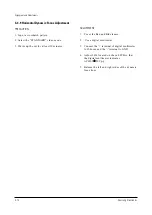
4-4-7 Static Focus Adjustment
PRECAUTION
1. Select the “STANDARD” video mode.
2. Input a crosshatch pattern.
3. Cover the lenses that are not being adjusted.
4. Connect a convergence jig and read data.
5. Adjust the lens for best focus.
(See Fig, 4-1, next page)
STATIC FOCUS (CONTINUED)
Vary the focus pack VR (Red, Blue) on the
front cabinet. Adjust the TV for best possible
focus around the center of the crosshatch
pattern, without losing overall screen balance.
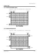
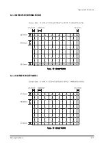
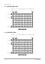
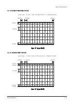
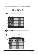
Figure Crosshatch Pattern
Examine these points together.
4-4-8 Lens Focus Adjustment
PRECAUTIONS
1. Do this adjustment after the static focus
adjustment and the tilt adjustment.
2. Select the “STANDARD” video mode.
(Contrast:100, Brightness:50)
3. Input a crosshatch pattern.
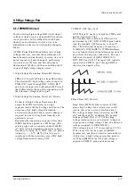
ADJUSTMENT
1. Loosen the lens screws.
2. Cover the two lenses that are not being
adjusted.
3. Adjust the lens, observing the color aberration
vertically and horizontally within 3 blocks of
the center of the crosshatch pattern.
4. When the lens is turned clockwise, the color
aberration will change as follows:
Lens
Color Aberration Change
R Orange - Crimson
G Blue - Red
B Purple - Green
5. Green
lens
adjustment:
Set the lens at the point where Blue just
changes to Red. If the color aberration is
irregular throughout the picture screen, adjust
the lens to show Red color aberration
(approximately 1~3 mm area) within a 3-block
grid around the horizontal center-line. If the
color aberration is irregular, adjust the lens as
shown in the diagram below. (Accurate
alignment of Green is important for overall
color quality.)
6. Red lens adjustment
Set the Red lens at the point where Orange
becomes Crimson.
7. Blue lens adjustment
Set the Blue lens at the point where Purple
becomes Green.
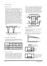
P
L1
L2
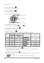
RED ABERRATION BLUE ABERRATION
L1, L2 < P
_
Fig. 4-1 Crosshatch Pattern.
Fig. 4-2 Color Aberration
Examine these points together
Содержание PCL545RX/XAA
Страница 2: ...ELECTRONICS Samsung Electronics Co Ltd AUG 2001 Printed in Korea AA68 ...
Страница 11: ...Reference Information Samsung Electronics 2 5 2 3 MICOM IIC BUS LINE UP ...
Страница 12: ...Reference Information 2 6 Samsung Electronics MENO ...
Страница 14: ...Specifications 3 2 Samsung Electronics MENO ...
Страница 30: ...Alignment and Adjustments 4 16 Samsung Electronics 4 6 3 PCL6215R NORMAL MODE 4 6 4 PCL6215R DTV MODE ...
Страница 31: ...Alignment and Adjustments Samsung Electronics 4 17 4 6 5 472W 4715W NORMAL MODE 4 6 6 472W 4715W DTV MODE ...
Страница 32: ...Alignment and Adjustments 4 18 Samsung Electronics 4 6 7 552W 5515W NORMLA MODE 4 6 8 552W 5515W DTV MODE ...
Страница 33: ...Alignment and Adjustments Samsung Electronics 4 19 4 6 9 652W 6515R NORMAL MODE 4 6 10 652W 6515R DTV MODE ...
Страница 38: ...Alignment and Adjustments 4 24 Samsung Electronics ...
Страница 39: ...Alignment and Adjustments Samsung Electronics 4 25 ...
Страница 40: ...Alignment and Adjustments 4 26 Samsung Electronics ...
Страница 41: ...Alignment and Adjustments Samsung Electronics 4 27 1 4 8 2 Perfect Focus Factory Mode ...
Страница 42: ...Alignment and Adjustments 4 28 Samsung Electronics 2 3 4 ...
Страница 58: ...Alignment and Adjustments 4 44 Samsung Electronics MENO ...
Страница 62: ...MEMO 5 4 Samsung Electronics ...
Страница 67: ...Exploded View Part List Samsung Electronics 6 5 6 5 HCL47WX XAA HCL4715WX XAA ...
Страница 69: ...Exploded View Part List Samsung Electronics 6 7 6 7 HCL552WX XAA HCL5515WX XAA ...
Страница 71: ...Exploded View Part List Samsung Electronics 6 9 6 9 HCL652WX XAA HCL6515WX XAA ...
Страница 162: ...7 90 Samsung Electronics MEMO ...
Страница 163: ...Samsung Electronics Block Diagrams 8 1 8 Block Diagram 8 1 Main Signal Progressive ...
Страница 164: ...Block Diagrams 8 2 Samsung Electronics 8 2 Video Signal ...
Страница 165: ...Samsung Electronics Block Diagrams 8 3 8 3 Sound Signal ...
Страница 168: ...Block Diagrams 8 6 Samsung Electronics 8 6 Simple PIP Applied IC CIA3250 SDA9400 Deflection Signal Processing ...
Страница 170: ...8 8 Video S W Signal Change Block Diagrams 8 8 Samsung Electronics ...
Страница 171: ...Samsung Electronics 8 9 D W Block Diagram SDA9400 Block Diagrams 8 9 Deflection Signal Processing ...
Страница 177: ...10 Schematic Diagrams Samsung Electronics Schematic Diagrams 10 1 10 1 MAIN 1 ...
Страница 178: ...Schematic Diagrams 10 2 Samsung Electronics 10 2 MAIN 2 ...
Страница 179: ...Samsung Electronics Schematic Diagrams 10 3 10 3 MAIN 3 TP02 TP01 TP01 TP02 ...
Страница 180: ...Schematic Diagrams 10 4 Samsung Electronics 10 4 MAIN 4 ...
Страница 181: ...Samsung Electronics Schematic Diagrams 10 5 10 5 MICOM TP04 TP03 TP03 TP04 ...
Страница 182: ...Schematic Diagrams 10 6 Samsung Electronics 10 6 POWER ...
Страница 183: ...Samsung Electronics Schematic Diagrams 10 7 10 7 SOUND ...
Страница 184: ...Schematic Diagrams 10 8 Samsung Electronics 10 8 CRT ...
Страница 185: ...Samsung Electronics Schematic Diagrams 10 9 10 9 3D COMB ...
Страница 186: ...Schematic Diagrams 10 10 Samsung Electronics 10 10 SUB 1 TP05 TP06 TP07 TP08 TP12 TP11 TP10 TP09 ...
Страница 188: ...Schematic Diagrams 10 12 10 11 SUB 2 TP14 TP13 TP13 TP14 ...
Страница 190: ...Schematic Diagrams 10 14 Samsung Electronics 10 13 A V TERMINAL ...
Страница 191: ...Samsung Electronics Schematic Diagrams 10 15 10 14 AV CONTROL ...
Страница 192: ...Schematic Diagrams 10 16 Samsung Electronics 10 15 CONVERGENCE TP18 TP19 TP20 TP21 TP22 TP23 ...
Страница 193: ...Samsung Electronics Schematic Diagrams 10 17 10 16 CONVERGENCE SDC11 1 ...
Страница 194: ...Schematic Diagrams 10 18 Samsung Electronics 10 17 CONVERGENCE SDC11 2 ...
Страница 195: ...Samsung Electronics Schematic Diagrams 10 19 10 18 PERFECT FOCUS PHOTO SENSOR INTERFACE BOARD ...
Страница 196: ...Schematic Diagrams 10 20 Samsung Electronics 10 19 CAPTION ...
Страница 197: ...Samsung Electronics Schematic Diagrams 10 21 10 20 AV FRONT ...
Страница 198: ...Schematic Diagrams 10 22 Samsung Electronics 10 21 CONTROL VM CONTROL VM ...
Страница 199: ...Samsung Electronics Schematic Diagrams 10 23 10 22 DW 1 ...
Страница 200: ...Schematic Diagrams 10 24 Samsung Electronics 10 23 DW 2 ...
Страница 201: ...Samsung Electronics Schematic Diagrams 10 25 10 24 DW 3 TP24 TP25 TP26 TP29 TP31 TP30 TP34 TP33 TP27 TP28 TP32 ...


