background image

SAMSUNG Proprietary-Contents may change without notice

This Document can not be used without Samsung's authorization

Flow Chart of Troubleshooting

9-21

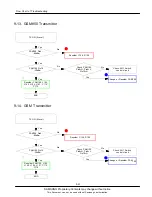
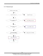
9-13. GSM850 Transmitter

9-14. GSM Transmitter

Change or Resolder PAM100

Yes

PAM100 Pin4

-65dBm

TX ON (5Level)

Check PAM100

Pin8=H, Pin9=L,

Pin10=H

PAM100 Pin15

-30dBm

Check ANT Switch

control circuit

Yes

Yes

Yes

No

No

No

END

Change or Resolder PAM100

Yes

PAM100 Pin4

-65dBm

TX ON (5Level)

Check PAM100

Pin8=H, Pin9=L,

Pin10=H

PAM100 Pin15

-30dBm

Check ANT Switch

control circuit

Yes

Yes

Yes

No

No

No

Resolder C126, R105

END

Resolder PAM100, L103,
L145, L104, L107, C115,

C170

Resolder PAM100, L103,
L145, L104, L107, C115,

C170

Resolder C126, R105

Содержание GT-C3510T

Страница 1: ...ns 2 Specification 3 Product Function 4 Array course control 5 Exploded View and Parts List 6 Main Electrical Parts List 7 Block Diagrams 8 PCB Diagrams 9 Flow Chart of Troubleshooting 10 Reference da...

Страница 2: ...e worn away Use a thicken twisted wire when you measure level A thicken twisted wire has low resistance therefore error of measurement is few Repair after separate Test Pack and Set because for short...

Страница 3: ...ned your body before you touch semiconductor or parts with semiconductor There are ways that you touch an earthed place or wear static electricity prevention string on wrist Use earthed soldering stee...

Страница 4: ...8 251 0 124 975 1023 512 885 512 810 Tx Rx spacing 45MHz 45MHz 95MHz 80MHz Mod Bit rate Bit Period 270 833kbps 3 692us 270 833kbps 3 692us 270 833kbps 3 692us 270 833kbps 3 692us Time Slot Period Fram...

Страница 5: ...9 12 4 dBm 10 10 4 dBm 11 8 4 dBm 12 6 4 dBm 13 4 4 dBm 14 2 5 dBm 15 0 5 dBm TX Power control level GSM850 GSM900 5 33 2 dBm 6 31 2 dBm 7 29 2 dBm 8 27 2 dBm 9 25 2 dBm 10 23 2 dBm 11 21 2 dBm 12 19...

Страница 6: ...out notice 3 Product Function 3 1 This Document can not be used without Samsung s authorization Main Function EDGE 1 3 Mega Pixel Camera GSM 850 900 1800 1900 Analog TV Music player Bluetooth FM Radio...

Страница 7: ...hange without notice 4 Array course control 4 1 This Document can not be used without Samsung s authorization Test Jig GH99 36900A 4 1 Software Adjustments Test Cable GH39 01313A RF Test Cable GH39 00...

Страница 8: ...nt can not be used without Samsung s authorization 4 2 Software Downloading 4 2 1 Pre requisite for Downloading Downloader Program Downloader V5 56 GT C3510T Mobile Phone Data Cable Binary file 4 2 2...

Страница 9: ...SAMSUNG Proprietary Contents may change without notice Array course control 4 3 This Document can not be used without Samsung s authorization 2 Select the BRCM2133 as Control...

Страница 10: ...SAMSUNG Proprietary Contents may change without notice Array course control 4 4 This Document can not be used without Samsung s authorization 3 Select the Full Download...

Страница 11: ...ontents may change without notice Array course control 4 5 This Document can not be used without Samsung s authorization 4 Load the file of Boot Apps Rsrc 1 Rsrc2 Factory FS from the folder that you s...

Страница 12: ...rol 4 6 This Document can not be used without Samsung s authorization 5 Click the Port Search button when the download cable is connected to PC cf You have to set the phone as a download mode by press...

Страница 13: ...SAMSUNG Proprietary Contents may change without notice Array course control 4 7 This Document can not be used without Samsung s authorization 6 Then the down loader can search the port...

Страница 14: ...not be used without Samsung s authorization 7 Click the Download button when the Port searched It will start to download 7 When downloading is finished successfully there is a All files complete messa...

Страница 15: ...SAMSUNG Proprietary Contents may change without notice 5 Exploded View and Parts List 5 1 This Document can not be used without Samsung s authorization 5 1 Cellular phone Exploded View...

Страница 16: ...I6230 GH59 09015A QSP01 MODULE GTI6230_SPK CARRIER GH59 09024A QME03 TOUCH PANEL GT C3510T BLK GH59 09160A QLB01 NDC BRACKET SHIELD GH71 09331A QMP01 A S ASSY GTC3510T_PBA MAIN SVC GH82 04811A QLC01 A...

Страница 17: ...01329 ZD105 DIODE TVS 0505 002207 U101 FET SILICON 0801 003026 U301 IC 0801 003130 U200 IC 1001 001546 U102 U300 IC 1108 000296 UME200 MEMORY 1201 002675 U302 IC 1201 002933 PAM100 IC 1203 006070 U400...

Страница 18: ...1 R217 R CHIP 2007 007156 R424 R CHIP 2007 008401 R205 R CHIP 2007 008517 R206 R CHIP 2007 008776 R411 R CHIP 2007 008780 R127 R128 R417 R419 R CHIP 2007 008780 R421 R CHIP 2203 000233 C110 C237 C358...

Страница 19: ...IP 2203 006048 C217 C218 C306 C308 C CERAMIC CHIP 2203 006048 C309 C311 C344 C345 C CERAMIC CHIP 2203 006048 C346 C355 C408 C411 C CERAMIC CHIP 2203 006048 C413 C417 C427 C432 C CERAMIC CHIP 2203 0062...

Страница 20: ...6 L112 L114 L137 L141 INDUCTOR SMD 2703 001726 L201 INDUCTOR SMD 2703 002170 L108 L109 INDUCTOR SMD 2703 002176 L118 L121 INDUCTOR SMD 2703 002200 L134 INDUCTOR SMD 2703 002203 L125 L127 INDUCTOR SMD...

Страница 21: ...L416 CORE FERRITE BEAD 3301 001812 L302 L303 L304 L305 CORE FERRITE BEAD 3301 001917 L123 L401 L402 L410 CORE FERRITE BEAD 3404 001303 TAC_CAM TAC_DN SWITCH TACT 3404 001303 TAC_HOLD TAC_UP SWITCH TA...

Страница 22: ...1 GPEN1 VC2 RF_INN_0G8 RF_INP_0G8 RF_INN_0G9 RF_INP_0G9 RF_INN_1G8 RF_INP_1G8 RF_INN_1G9 RF_INP_1G9 AUXDACOUT GPEN6 TX_EN RF_PA_LB LB_TX RF_PA_HB HB_RX PAM VC1 GPCTRL0 VC2 GPCTRL1 LB_RX RX0 HB_RX RX1...

Страница 23: ...264 WMV9 MPEG4 MP3 AAC AAC eAAC WMA 64 Poly MIDI SPK AMP 400mW HEADSET AMP 100mW I2S SPI PCM USIM Interface Bluetooth FM Key 3X1 CAM HOLD VOL_UP VOL_DN Memory NAND 2Gbit DDRAM 1Gbit LARGE BLOCK SIM Ca...

Страница 24: ...Top 0 0 2 C 1 0 2 C 4 0 2 C C205 C206 7 0 2 C C216 9 1 2 C 0 2 2 C 1 2 2 C 3 2 2 C 4 2 2 C 0 3 2 C C413 C429 0 4 4 C 1 4 4 C C442 3 4 4 C C449 C450 C451 2 5 4 C CLR 5 0 4 D 6 0 4 D D NE F404 HDC402 0...

Страница 25: ...448 3 5 4 C D300 D400 D402 D403 0 0 4 R A E 0 0 1 F F101 F102 F400 F401 F402 0 0 4 C D H 1 0 4 C D H 0 0 4 C F I 0 0 1 L 1 0 1 L 2 0 1 L L103 L104 L105 L106 L107 L108 L109 L110 L111 L112 3 1 1 L L114...

Страница 26: ...not work Yes Yes No Download again Check the VBAT more than 3 3V No Check the Battery Yes Check the related circuit No C304 VBAT 3 0V Yes Check the PM300 and L301 No Check the VDD_MEM_1 8V of PM300 i...

Страница 27: ...B1 PGND2 B2 O D L M I S 3 B 3 N I 4 B C N 1 C N 2 C N 1 A 1 X L 2 A 1 N I 3 A O D L O I 4 A 2 O D L C H 5 A 5 3 3 C 0 0 3 M P 0 0 3 T A B 6 0 3 C 3 0 3 C 8 2 3 C 6 4 3 C 3 1 3 C 0 1 3 C 4 4 3 C 1 1 3...

Страница 28: ...is Document can not be used without Samsung s authorization Flow Chart of Troubleshooting 9 3 9 2 Initial Initial Failure Yes PM300 pin E3 RESETB H check the test point No Check the circuit related to...

Страница 29: ...B1 PGND2 B2 O D L M I S 3 B 3 N I 4 B C N 1 C N 2 C N 1 A 1 X L 2 A 1 N I 3 A O D L O I 4 A 2 O D L C H 5 A 5 3 3 C 0 0 3 M P 0 0 3 T A B 6 0 3 C 3 0 3 C 8 2 3 C 6 4 3 C 3 1 3 C 0 1 3 C 4 4 3 C 1 1 3...

Страница 30: ...s authorization Flow Chart of Troubleshooting 9 5 9 3 Charging Part Yes Resolder or replace PM300 Check the circuit related to ACC_DET signal Check the circuit related to VBUS_5V_IF Yes No Check the P...

Страница 31: ...B1 PGND2 B2 O D L M I S 3 B 3 N I 4 B C N 1 C N 2 C N 1 A 1 X L 2 A 1 N I 3 A O D L O I 4 A 2 O D L C H 5 A 5 3 3 C 0 0 3 M P 0 0 3 T A B 6 0 3 C 3 0 3 C 8 2 3 C 6 4 3 C 3 1 3 C 0 1 3 C 4 4 3 C 1 1 3...

Страница 32: ...Chart of Troubleshooting 9 7 9 4 Sim Part Phone can t access SIM Card Yes Check the VDD_SIM_3 0V 3 0V No Check the circuit related to C362 Yes Check the SIM connector s connector s to SIM card resold...

Страница 33: ...1 1 2 C 3 1 5 1 3 C 2 1 5 C 6 C 4 1 7 C 6 1 0 0 3 M I S 3 1 2 4 3 5 6 4 5 7 8 6 0 6 3 C V 3 3 _ D S _ D D V 6 5 0 3 D Z 1 2 3 4 5 2 1 3 R 5 1 3 R 3 6 3 C V 0 3 _ G I D _ D D V 7 1 3 R 9 5 3 C 8 2 3 R...

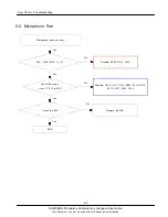
Страница 34: ...msung s authorization Flow Chart of Troubleshooting 9 9 9 5 Microphone Part Microphone does not work Yes Resolder R409 R414 C439 C421 MIC_BIAS H No Yes Resolder C408 C411 C410 R409 R410 R414 R415 C427...

Страница 35: ...I M 0 1 4 R 9 3 4 C D403 0 3 4 C 1 1 4 C 9 0 4 C 9 0 4 L 8 2 4 C 4 1 4 C 5 0 4 C D402 2 1 4 L 4 1 4 R 2 3 4 C 6 1 4 R 3 0 4 R 7 2 4 C 2 1 4 C S A I B _ C I M 5 1 4 R 0 1 4 C 4 2 4 L 5 0 4 L P _ C I M...

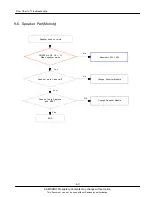
Страница 36: ...ut Samsung s authorization Flow Chart of Troubleshooting 9 11 9 6 Speaker Part Melody Speaker does not work PM300 pin G9 J8 H When speaker works Resolder L302 L303 No Yes No Change Receiver Module Doe...

Страница 37: ...N 2 C N 1 A 1 X L 2 A 1 N I 3 A O D L O I 4 A 2 O D L C H 5 A 5 3 3 C 0 0 3 M P 0 0 3 T A B 6 0 3 C 3 0 3 C 8 2 3 C 6 4 3 C 3 1 3 C 0 1 3 C 4 4 3 C 1 1 3 C 6 1 3 C 7 2 3 C 7 0 3 C 4 0 3 R 1 3 3 C 8 1...

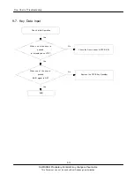
Страница 38: ...ut Samsung s authorization Flow Chart of Troubleshooting 9 13 9 7 Key Data Input Check Initial Operation Yes When one of the keys is pushed is it displayed on LCD Check the Dome sheet FPCB KEY No Yes...

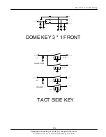
Страница 39: ...R F 1 3 Y E K E M O D E M U L O V 8 3 4 C ZD402 5 3 4 C D N E 1 2 D N E S 1 2 3 0 4 D Z 3 4 5 6 7 1 2 N D _ C A T 7 3 4 C 5 6 7 1 2 D L O H _ C A T 3 4 6 7 1 2 P U _ C A T 3 4 5 R L C 1 2 4 0 4 D Z 6...

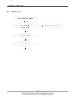
Страница 40: ...ent can not be used without Samsung s authorization Flow Chart of Troubleshooting 9 15 9 8 Camera part Camera function does not work Yes Check the Camera connector on PBA Reconnect the camera module N...

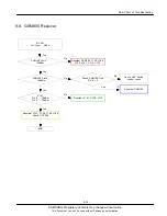
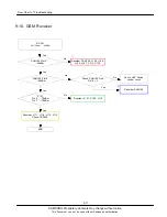
Страница 41: ...tion 9 16 9 9 GSM850 Receiver RX ON Cell Power 60dBm PAM100 Pin15 65dBm Yes Resolder PAM100 L103 L145 L104 L107 C115 C170 No Yes No Check PAM100 Pin9 Pin10 L PAM100 Pin18 68dBm Check ANT Switch contro...

Страница 42: ...oting 9 17 9 10 GSM Receiver PAM100 Pin15 65dBm Yes Resolder PAM100 L103 L145 L104 L107 C115 C170 No Yes No Check PAM100 Pin9 Pin10 L PAM100 Pin18 68dBm Check ANT Switch control circuit No Yes Resolde...

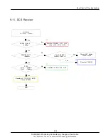
Страница 43: ...tion 9 18 9 11 DCS Receiver Yes No Resolder F102 C140 L119 F102 Pin 8 70dBm Pin 9 70dBm Yes Resolder PAM100 Yes No Check ANT Switch control circuit Check PAM100 Pin9 H Pin10 L No Yes No Resolder PAM10...

Страница 44: ...ting 9 19 9 12 PCS Receiver Yes PAM100 Pin15 65dBm Resolder PAM100 L103 L145 L104 L107 C115 C170 No Yes Check ANT Switch control circuit PAM100 Pin17 68dBm Check PAM100 Pin9 H Pin10 L No No Resolder P...

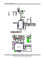
Страница 45: ...R T C P G C N 2 1 NC 16 9 1 C N 2 RFIN_HB 4 RFIN_LB 0 X R D N G 3 2 D N G 4 2 D N G GND 14 D N G 3 D N G 5 D N G 6 3 1 D N G GND 0 0 1 M A P ANT 15 1 D N G 1 2 D N G 2 2 7 2 1 L 8 0 1 L 2 1 1 L 3 0 1...

Страница 46: ...n4 65dBm TX ON 5Level Check PAM100 Pin8 H Pin9 L Pin10 H PAM100 Pin15 30dBm Check ANT Switch control circuit Yes Yes Yes No No No END Change or Resolder PAM100 Yes PAM100 Pin4 65dBm TX ON 5Level Check...

Страница 47: ...Resolder C125 R104 Yes Check ANT Switch control circuit PAM pin14 30dBm Check PAM100 Pin8 H Pin9 H Pin10 H No No Change or Resolder PAM100 Yes Yes END TX ON 5Level Yes PAM100 Pin31 65dBm No Yes Check...

Страница 48: ...B 0 X R D N G 3 2 D N G 4 2 D N G GND 14 D N G 3 D N G 5 D N G 6 3 1 D N G GND 0 0 1 M A P ANT 15 1 D N G 1 2 D N G 2 2 3 0 1 L 3 0 1 R 7 0 1 P T 5 2 1 C 5 1 1 C 6 2 1 C 2 0 1 T N A 8 0 1 P T 0 7 1 C...

Страница 49: ...ization 9 24 9 17 Bluetooth part Bluetooth connection disable Yes Check BT function ON Enable BT function No Yes Check the voltage of C100 is around 3 0V No Check PM300 and change Check 26MHz Clock on...

Страница 50: ...U C4 VSS A5 FM_VDDAUDIO SPARE A6 7 A E R A P S 8 A P X R _ M F 1 B N _ S T R _ T R A U 2 B 5 O I P G 3 B L _ T U O A _ M F 4 B R _ T U O A _ M F 0 0 1 U 1 NC 2 NC 1 A Q R I _ M F 6 O I P G 2 A E D O...

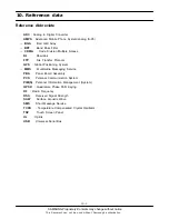
Страница 51: ...CDMA Code Division Multiple Access DL Downlink FTP File Transfer Protocol GPS Global Positioning System MMS Multimedia Messaging Service PBA Panel Board Assembly PCS Personal Communication System PIM...

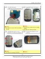
Страница 52: ...n 1 Be careful not to make scratch and molding damage Caution 1 Be careful not to make damage to INTENNA Caution 1 Be careful not to make scratch and molding damage 1 Unscrew the 6 points 1 1 Perform...

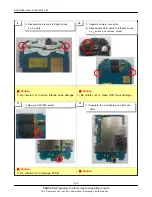
Страница 53: ...ding damage Caution 1 Be careful not to make scratch and molding damage 2 Be careful not to damage the PBA Caution 1 Be careful not to damage LCD FPCB Caution 5 6 7 8 1 After lifting PBA upward disass...

Страница 54: ...ful not to make intenna hook damage Caution 1 Be careful not to make SPK Hook damage Caution 1 Be careful not to damage FPCB Caution 9 10 11 12 1 Disassemble intenna s left right hooks on 2 points 1 S...

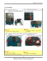
Страница 55: ...Caution 1 Be careful not to damage the receiver FPCB SPK WIRE Caution 1 Confirm receiver s location 2 Be careful not to make SPK Hook damage Caution 1 Be careful not to damage PBA 11 2 Assembly 1 2 3...

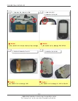
Страница 56: ...s authorization Caution 1 Be careful not to make Intenna hook damage Caution 1 Be careful not to damage TSP FPCB Caution 1 Be careful not to damage LCD Caution 1 Be careful not to damage to LCD conne...

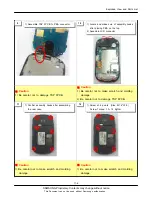
Страница 57: ...and molding damage 2 Be careful not to damage TSP FPCB Caution 1 Be careful not to make scratch and molding damage Caution 1 Be careful not to make scratch and molding damage 9 10 11 12 1 Assemble TSP...

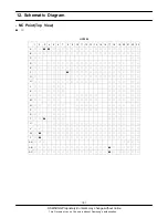
Страница 58: ...without notice 12 Schematic Diagram 12 1 This Document can not be used without Samsung s authorization NC Point Top View NC UCP200 1 2 3 4 5 6 7 8 9 10 11 12 13 14 15 16 17 18 19 20 21 22 23 A B C D E...

Страница 59: ...prietary Contents may change without notice Schematic Diagram 12 2 This Document can not be used without Samsung s authorization PM300 1 2 3 4 5 6 7 8 9 A B C D E F G H J U100 1 2 3 4 5 6 7 8 9 A B C...

Страница 60: ...UNG Proprietary Contents may change without notice Schematic Diagram 12 3 This Document can not be used without Samsung s authorization UME200 1 2 3 4 5 6 7 8 9 10 11 12 13 14 A B C D E F G H J K L M...

Страница 61: ...0 5 1 C 2 3 1 C 2 1 1 L 3 4 1 L 3 0 1 L 7 1 1 R 2 5 1 C 7 4 1 C 4 4 5 5 3 0 1 R 7 0 1 C S 1 1 2 2 3 3 6 2 1 R 0 2 1 R L123 V 8 2 _ O I _ M A C _ D D V 5 2 1 L 0 1 1 L 5 1 1 L 4 4 5 5 1 0 1 H B 1 0 1 C...

Страница 62: ...D C L 4 1 D 5 Q D A F 5 1 D 6 1 D 9 Q D A F 1 1 Q D A F 7 1 D 2 1 Q D A F 8 1 D 9 1 D 3 1 Q D A F RF_VSS D2 1 C RF_VSS C2 P W F 2 2 C N V D A F 3 2 C 9 G 0 _ P N I _ F R 1 D 8 N E P G 0 1 D 1 1 D 6 N...

Страница 63: ...C 2 O D L C H 6 A 1 O D L C H 7 A 2 O D L F R 8 A 1 O D L F R 9 A C N B1 PGND1 B2 PGND2 3 B O D L M I S 4 B 1 C N 2 C N 1 A C N 2 A 1 X L 3 A 1 N I 4 A O D L O I 5 A 0 0 3 M P 5 3 3 C 7 5 3 C C N 4 5...

Страница 64: ...2 1 2 2 2 2 2 3 3 1 1 0 1 0 1 1 1 1 1 2 1 2 1 3 1 3 1 4 1 4 1 5 1 5 1 6 1 6 1 0 0 4 C D H 1005 9 0 4 C F P 5 1 V 0 5 0 0 4 D A P C I M C I M 0 3 2 6 I T G 6 0 4 L 5 1 4 L 4 1 4 L 5 2 4 C 0 1 4 R K 2...

Страница 65: ...ngportal com Europe europe samsungportal com China china samsungportal com Asia asia samsungportal com Mideast Africa mea samsungportal com This Service Manual is a property of Samsung Electronics Co...

Отзывы: