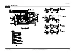


Circuit Operating Descriptions
Samsung Electronics
13-5
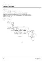
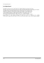
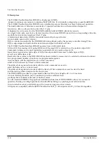
13-3-4 Transport stream processing
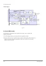
The STi5100/STi5101 supports dual independent transport stream inputs using an SRAM-based
packet merger and a single programmable transport interface (PTI). The merger
buffers a packet tagged with a source ID and a time stamp.
The merger is able to produce an output stream (1394) from the PTI alternate output or
the SWTS interface which is an STBus target normally fed by the central DMA. The
outgoing packets are buffered in the merger and are presented to the output pins using a
dejittering mechanism that compares each packet time stamp with a fixed programmable
offset.
The PTI alternate output allows the entire transport stream or selected packets to be
output through the merger to an external device such as an IEEE1394 link layer controller.
The TS0IN input is by default a serial transport input. However, it may be extended to a
full parallel input by using additional PIO pins (alternatively used as the second smartcard
interface).
Multiplexing in front of the merger block provides a bypass route to allow for CableCard
and DVB-CI support. This provides a parallel loop back path between TS0 and TS2 where
the normally serial TS0 is augmented using PIO bits. If the TS0 input is serial only then
the loopback path can still be provided but is done inside the merger block which performs
the serial to parallel conversion. This allows a serial-only front-end to be used with DVB-CI.
TS1IN is a fully parallel input that may accept a standard transport stream or D1 raw data.
An internal multiplexor routes this to the stream merger’s upper port, which has an internal
by-pass directly to the PTI. D1 header processing and buffering is performed by the PTI.
Transport deMUX and D1 processing may not be performed simultaneously.
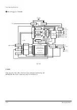
1) Block diagram: Transport stream merger inputs and outputs
fig. 13-4
Содержание DSB-S300G
Страница 13: ...3 2 Software Update Samsung Electronics MEMO ...
Страница 19: ...4 6 Disassembly and Reassembly Samsung Electronics MEMO ...
Страница 30: ...Samsung Electronics 6 1 6 Exploded View and Parts List 6 1 Ass y Chassis 6 2 ...
Страница 33: ...Exploded View and Parts List 6 4 Samsung Electronics MEMO ...
Страница 46: ...9 1 9 Wiring Diagram Samsung Electronics ...
Страница 47: ...Wiring Diagram 9 2 MEMO Samsung Electronics ...
Страница 48: ...10 1 10 PCB Diagrams 10 1 Main PCB 10 2 Front PCB 10 3 S M P S PCB 10 2 10 5 10 6 Samsung Electronics ...
Страница 51: ...PCB Diagrams 10 4 Samsung Electronics CONDUCTOR SIDE ...
Страница 52: ...PCB Diagrams 10 5 Samsung Electronics 10 2 Front PCB COMPONENT SIDE CONDUCTOR SIDE ...
Страница 53: ...PCB Diagrams 10 6 Samsung Electronics 10 3 S M P S PCB COMPONENT SIDE ...
Страница 54: ...PCB Diagrams 10 7 Samsung Electronics CONDUCTOR SIDE ...
Страница 55: ...PCB Diagrams 10 8 Samsung Electronics MEMO ...
Страница 69: ...Schematic Diagrams 11 14 Samsung Electronics MEMO ...
Страница 70: ...Samsung Electronics 12 1 12 Operating Instructions ...
Страница 71: ...Operating Instructions 12 2 Samsung Electronics ...
Страница 72: ...Operating Instructions 12 3 Samsung Electronics ...
Страница 73: ...Operating Instructions 12 4 Samsung Electronics ...
Страница 74: ...Operating Instructions 12 5 Samsung Electronics ...
Страница 75: ...Operating Instructions 12 6 Samsung Electronics ...
Страница 97: ...Circuit Operating Descriptions 13 22 Samsung Electronics MEMO ...


