1-3
Precautions
Samsung Electronics
5. Check the insulation between the blades of
the AC plug and accessible conductive parts
(examples: metal panels, input terminals
and earphone jacks).
6. Insulation Checking Procedure: Disconnect
the power cord from the AC source and
turn the power switch ON. Connect an
insulation resistance meter (500V) to the
blades of the AC plug.
The insulation resistance between each
blade of the AC plug and accessible
conductive parts (see above) should be
greater than 1 megohm.
7. Never defeat any of the B+ voltage
interlocks. Do not apply AC power to the
unit (or any of its assemblies) unless all
solid-state heat sinks are correctly installed.
8. Always connect a test instrument's ground
lead to the instrument chassis ground
before
connecting the positive lead; always
remove the instrument's ground lead last.
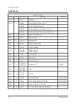
1-3 Precautions for Electrostatically Sensitive Devices (ESDs)
1. Some semiconductor ("solid state") devices
are easily damaged by static electricity.
Such components are called Electrostatically
Sensitive Devices (ESDs); examples include
integrated circuits and some field-effect
transistors. The following techniques will
reduce the occurrence of component
damage caused by static electricity.
2. Immediately before handling any
semiconductor components or assemblies,
drain the electrostatic charge from your
body by touching a known earth ground.
Alternatively, wear a discharging
wrist-strap device. (Be sure to remove it
prior to applying power--this is an electric
shock precaution.)
3. After removing an ESD-equipped assembly,
place it on a conductive surface such as
aluminum foil to prevent accumulation of
electrostatic charge.
4. Do not use freon-propelled chemicals.
These can generate electrical charges that
damage ESDs.
5. Use only a grounded-tip soldering iron
when soldering or unsoldering ESDs.
6. Use only an anti-static solder removal
device. Many solder removal devices are
not rated as "anti-static"; these can
accumulate sufficient electrical charge to
damage ESDs.
7. Do not remove a replacement ESD from its
protective package until you are ready to
install it. Most replacement ESDs are
packaged with leads that are electrically
shorted together by conductive foam,
aluminum foil or other conductive
materials.
8. Immediately before removing the protective
material from the leads of a replacement
ESD, touch the protective material to the
chassis or circuit assembly into which the
device will be installed.
9. Minimize body motions when handling
unpackaged replacement ESDs. Motions
such as brushing clothes together, or lifting
a foot from a carpeted floor can generate
enough static electricity to damage an ESD.
WARNING1:
First read the "Safety Precautions" section of this manual. If some unforeseen circumstance creates a conflict
between the servicing and safety precautions, always follow the safety precautions.
WARNING2: An electrolytic capacitor installed with the wrong polarity might explode.
1-2 Servicing Precautions
1. Servicing precautions are printed on the
cabinet. Follow them.
2. Always unplug the unit's AC power cord
from the AC power source before
attempting to: (a) Remove or reinstall any
component or assembly, (b) Disconnect an
electrical plug or connector, (c) Connect a
test component in parallel with an
electrolytic capacitor.
3. Some components are raised above the
printed circuit board for safety. An
insulation tube or tape is sometimes used.
The internal wiring is sometimes clamped to
prevent contact with thermally hot
components. Reinstall all such elements to
their original position.
4. After servicing, always check that the
screws, components and wiring have been
correctly reinstalled. Make sure that the
portion around the serviced part has not
been damaged.
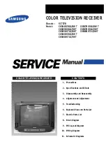
Содержание CK564BZR1X/BWT
Страница 2: ...ELECTRONICS Samsung Electronics Co Ltd MAY 1998 Printed in Korea 3SCT57B 6604 ...
Страница 13: ...3 4 Samsung Electronics MEMO MEMO ...
Страница 25: ...4 12 Samsung Electronics MEMO MEMO ...
Страница 45: ...PCB Layout 9 2 Samsung Electronics 9 2 PCB A V 9 5 PCB PIP 9 3 PCB NICAM 9 6 PCB TTX 9 4 PCB STEREO ...
Страница 47: ...Schematic Diagrams 11 1 Samsung Electronics 11 Schematic Diagrams 11 1 MAIN POWER ...
Страница 48: ...Schematic Diagrams 11 2 Samsung Electronics 11 2 MAIN CHROMA ...
Страница 49: ...Schematic Diagrams 11 3 Samsung Electronics 11 3 MAIN AUDIO ...
Страница 50: ...Schematic Diagrams 11 4 Samsung Electronics 11 4 MAIN U COM ...
Страница 51: ...Schematic Diagrams 11 5 Samsung Electronics 11 5 MAIN CRT ...
Страница 52: ...Schematic Diagrams 11 6 Samsung Electronics 11 6 STEREO SIF ...
Страница 53: ...Schematic Diagrams 11 7 Samsung Electronics 11 7 MAIN NICAM ...
Страница 54: ...Schematic Diagrams 11 8 Samsung Electronics 11 8 PIP TTX ...
Страница 55: ...Schematic Diagrams 11 9 Samsung Electronics 11 9 TTX OPTION ...
Страница 56: ...Schematic Diagrams 11 10 Samsung Electronics 11 10 PCB A V ...

