Alignment and Adjustments
4-8
Samsung Electronics
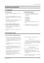
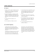
4-3-4 FOCUS Adjustment
1. Input a black and white signal.
2. Adjust the tuning control for the clearest
picture.
3. Adjust the FOCUS control for well defined
scanning lines in the center area of the screen.
4-3-6 Purity Adjustment
1. Warm up the receiver for at least 20 minutes.
2. Plug in the CRT deflection yoke and tighten
the clamp screw.
3. Plug the convergence yoke into the CRT and
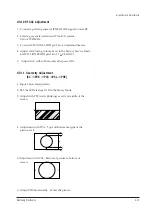
set in as shown in Fig. 4-1.
4. Input a black and white signal.
5. Fully demagnetize the receive by applying an
external degaussing coil.
6. Turn the CONTRAST and BRIGHTNESS
controls to maximum.
7. Loosen the clamp screw holding the yoke.
Slide the yoke backward or forward to provide
vertical green belt. (Fig. 4-2).
8. Tighten the convergence yoke.
9. Slowly move the deflection yoke forward, and
adjust for the best overall green screen.
10. Temporarily tighten the deflection yoke.
11. Produce blue and red rasters by adjusting the
low-light controls. Check for good purity in
each field.
12. Tighten the deflection yoke.
4-3-5 Screen Adjustment
1. Connect CRT socket pin RK to an oscilloscope
probe.
2. Input a gray scale pattern. (Use a pattern
generator, PM5518)
3. Use the P mode key (on the remote control) for
the STANDARD picture.
4. Adjust the Screen VR (on the FBT) so that the
voltage (See Fig.4-1.) on the oscilloscope
becomes 130 + 2.5V.
4-3-3 High Voltage Check
1. Connect a digital voltmeter to the second anode
of the picture tube.
2. Turn on the TV. Set the Brightness and
Contrast controls to minimum (zero beam
current).
3. The high voltage should not exceed 30KV.
4. Adjust the Brightness and contrast controls to
both extremes. Ensure that the high voltage
does not exceed 30KV under any conditions.
CAUTION: There is no high voltage adjustment on this
chassis. The B+ power supply must be set to +130/155
volts. (Full color bar input and normal picture level).
Fig. 4-1
130V 2.5Vp-p
_
+
GND
H-Blanking
Содержание CK564BZR1X/BWT
Страница 2: ...ELECTRONICS Samsung Electronics Co Ltd MAY 1998 Printed in Korea 3SCT57B 6604 ...
Страница 13: ...3 4 Samsung Electronics MEMO MEMO ...
Страница 25: ...4 12 Samsung Electronics MEMO MEMO ...
Страница 45: ...PCB Layout 9 2 Samsung Electronics 9 2 PCB A V 9 5 PCB PIP 9 3 PCB NICAM 9 6 PCB TTX 9 4 PCB STEREO ...
Страница 47: ...Schematic Diagrams 11 1 Samsung Electronics 11 Schematic Diagrams 11 1 MAIN POWER ...
Страница 48: ...Schematic Diagrams 11 2 Samsung Electronics 11 2 MAIN CHROMA ...
Страница 49: ...Schematic Diagrams 11 3 Samsung Electronics 11 3 MAIN AUDIO ...
Страница 50: ...Schematic Diagrams 11 4 Samsung Electronics 11 4 MAIN U COM ...
Страница 51: ...Schematic Diagrams 11 5 Samsung Electronics 11 5 MAIN CRT ...
Страница 52: ...Schematic Diagrams 11 6 Samsung Electronics 11 6 STEREO SIF ...
Страница 53: ...Schematic Diagrams 11 7 Samsung Electronics 11 7 MAIN NICAM ...
Страница 54: ...Schematic Diagrams 11 8 Samsung Electronics 11 8 PIP TTX ...
Страница 55: ...Schematic Diagrams 11 9 Samsung Electronics 11 9 TTX OPTION ...
Страница 56: ...Schematic Diagrams 11 10 Samsung Electronics 11 10 PCB A V ...

