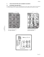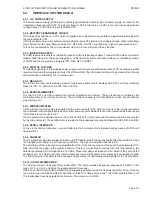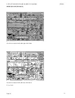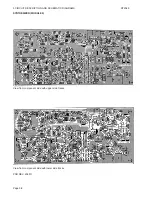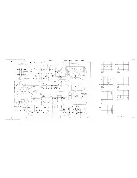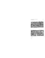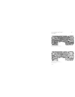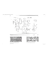
5.3. SYNTHESIZER UNIT (MODULE 3)
5.3.1. VCO with Buffer
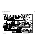
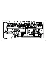
The voltage controlled oscillator, built around the Field Effect Transistor Q18, is oscillating either on the transmitting
frequency or on the first receiver local oscillator frequency, which means the receiving frequency less 15.3 MHz.
To reach this function, the oscillator is implemented with a bandshift by means of the bandswitch diode D6 and the
two capacitors C47 and C78.
In transmit mode, where the diode D6 is reverse biased, the oscillating frequency is mainly determined by C48, L9,
C49, C51, and D9.
In receiving mode the oscillator resonance frequency is lowered 15.3 MHz by switching D6 on and thus putting C47
and C78 in parallel with C48.
The oscillating frequency is varied by means of the control voltage fed to the capacitor diode D9.
The output voltage from the VCO is taken via a capacitive tap C52, C53 on the source of Q18 and fed to the common
buffer amplifier, built around Q15. The power gain of this stage is adjusted by means of potentiometer R98. The
gain is adjusted so that the output level from the TX buffer amplifier is 200 mW measured at the output connector J4.
5.3.2. loop Buffer Amplifier
The output from the common VCO buffer is fed to the divider chain via the stage around Q7, which secures the
needed amplification and the reverse isolation between the digital parts and the VCO.
The amplifier is a fixed tuned broad band amplifier with 11, C24, and R47 forming a low Q tuned circuit.
5.3.3. 32/33 Prescaler
The integrated circuit U4 is a two modulus prescaler based on the ECL technique.
From the Control logic in the programmable divider U3 pin 12, a high or low level is led to the prescaler U4 pin I.
A high level at U4 pin 1 causes the prescaler to divide by 33 and in turn a low level at pin I sets it up for dividing by 32.
The resistor R20 and the diode D4 work as a speed-up and overdrive protection circuit.
5.3.4. Reference/Programmable Divider and Phase Detector
The integrated circuit U3 comprises both a programmable divider for the reference input and a programmable
divider with control logic for use in conjunction with a dual modulus prescaler. Besides, the IC includes two phase
detectors and a lock detector of which only one of the phase detectors is in use, the output pins located at pin 15
and pin 16.
Both dividers are programmed via the serial bus from the microcomputer. The coding structure of the serial data
stream includes the needed information for the on-chip decoder to detect the kind of the reached division figures.
The reference division ratio is constant as the input of 3.7125 MHz is derived from the X-tal oscillator.
In the beginning of a counting period the prescaler U4 starts dividing by 33. After a few counts the modulus control
pin changes level and the prescaler will finish the dividing cycles with a division ratio of 32, ending up with the correct
total division ratio.
The pulse frequency out of the reference divider is 12.5 kHz. If the VCO frequency is correct the pulse frequency
from the variable divider is also 12.5 kHz and in phase with the pulse from the reference divider. The on-chip phase
detector compares the phase of the two pulses. If they are out of phase the detector creates correction pulses to
the Charge Pumpe for correction of the VCO frequency/phase.
However, the synthesizer circuit is made with a small constant phase error, forced by the current drawn through
R58, to avoid phase detector non linearities to degrade the loop performance. So the phase detector is sending
small correction pulses to transistor Q4 with a frequency of 12.5 kHz.
5.3.5. Charge Pumpe
The charge pumpe, mainly consisting of Q4, Q5, and D2, converts the pulse with modulated phase detector outputs
of U3 pin 15 and 16 to a DC current flowing into or out of the loop amplifier.
Assume that the VCO frequency has decreased from its nominal value. The phase detector will produce a negative
correction pulse on pin 16, turning Q5 on, resulting in current being drawn out of the loop amplifier.
This action will cause the output voltage to increase, thus increasing the VCO frequency to the nominal value.
An increase in VCO frequency from its nominal value will in turn cause a correction pulse on pin 15, turning Q4 off,
resulting in current flowing into the loop amplifier through the diode D2. This means the output voltage will decrease,
forcing the VCO frequency to decrease.
Because of the current drawn through R58, a small correction pulse of about 500 nsec. will always be present at
pin 15 on U3 with a frequency of 12.5 kHz.
5.3.6. Loop Amplifier/Filter
The loop amplifier is realized as a discrete operational amplifier with transistors Q10 and Q11 forming the input
differential pair and Q8, Q9 the output stage.
The loop dynamic performance is mainly controlled via the feed-back components in the loop amplifier, this means
5 CIRCUIT DESCRIPTION AND SCHEMATIC DIAGRAMS
RT2048
Page 5-6
0820
Содержание RT2048 VHF
Страница 1: ...INSTALLATION MANUAL SAILOR RT2048 VHF ...
Страница 4: ......
Страница 11: ...1 INTRODUCTION RT2048 Page 1 7 9403 BLOCK DIAGRAM ...
Страница 12: ......
Страница 22: ...2 INSTALLATION RT2048 Page 2 10 9346 626945 625473 ...
Страница 24: ...2 INSTALLATION RT2048 2 8 REAR VIEW OF VHF RT2048 25567 9350 Page 2 11 ...
Страница 26: ......
Страница 31: ...3 Service RT2048 3 10 PIN CONFIGURATIONS Page 3 5 ...
Страница 32: ...3 SERVICE RT2048 Page 3 6 ...
Страница 33: ...3 Service RT2048 Page 3 7 ...
Страница 34: ...3 SERVICE RT2048 Page 3 8 ...
Страница 38: ...5 CIRCUIT DESCRIPTION AND SCHEMATIC DIAGRAMS RT2048 Page 5 2 ...
Страница 89: ......
Страница 90: ...Thrane Thrane A S info thrane com www thrane com M2048GB Issue E 0820 ...

