


UPS25 6
RTD Embedded Technologies, Inc
List of Illustrations and Tables
.............................................................................................................................................................. Illustrations
Fig. 2-1 UPS25 Board layout showing jumper locations
Fig. 2-2 Base address jumpers illustrating address 300h
Fig. 2-3 Interrupt jumpers from left to right: IRQ 2,5,7,10,11,12,15
Fig. 2-4 Charger control, solder blobs, located near the left side of the PC/104
bus connector
Fig. 3-1 UPS25 integrated in a RTD PC/104 cpuModule stack together with a
HPWR104 power supply module
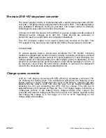
Fig. 3-2 UPS25 power supply connections
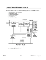
Fig. 4-1 Block diagram of the UPS25
Fig. 4-2 Discharging jumper
Fig. 4-3 Charger configuration, solder blobs B2 and B3
Fig. 4-4 Trip point adjustment trim pots for VIN and BATT levels
Fig. 4-5 I/O interface connector
...................................................................................................................................................................... Tables
Table 2-1 Factory configured jumper settings
Table 2-2 Base address jumper settings UPS25
Table 4-1 Charger status LED functional description
Table 4-2 I/O connector pin outs
Содержание UPS25
Страница 39: ...UPS25 39 RTD Embedded Technologies Inc...


