background image


RF-BM-ND08 

www.szrfstar.com

                                                                                                                                                  V1.2 - Sep., 2020 

Shenzhen RF-star Technology Co., Ltd.                                                                                                                   

Page  15  of  19


The module has two antenna output modes, which are on-board PCB antenna and stamp half-hole output (ANT pin, 

see pin function table for details). 

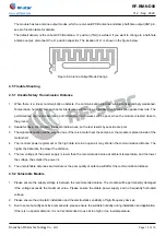
The default delivery is the onboard PCB antenna, L1 position (1NH) is welded. If you want to change to a half-hole 

antenna output, disconnect the L1 position capacitor. The location of L1 is shown in the figure below. 

Figure 8. Antenna Output Mode Change 

4.5 Trouble Shooting 

4.5.1 Unsatisfactory Transmission Distance   

1. 

When there is  a linear communication obstacle, the communication  distance will be correspondingly  weakened. 

Temperature, humidity, and co-channel interference will lead to an increase in communication packet loss rate. The 

performances of ground absorption and reflection of radio waves will be poor, when the module is tested close to 

the ground. 

2. 

Seawater has a strong ability to absorb radio waves, so the test results by seaside are poor. 

3. 

The signal attenuation will be very obvious, if there is a metal near the antenna or the module is placed inside of the 

metal shell. 

4. 

The incorrect power register set or the high data rate in an open air may shorten the communication distance. The 

higher the data rate, the closer the distance. 

5. 

The low voltage of the power supply is lower than the recommended value at ambient temperature, and the lower 

the voltage, the smaller the power is. 

6. 

The unmatchable antennas and module or the poor quality of antenna will affect the communication distance. 

4.5.2 Vulnerable Module 

1. 

Please ensure the supply voltage is between the recommended values. The module will be permanently damaged 

if the voltage exceeds the maximum value. Please  ensure the stable power supply and no frequently fluctuated 

voltage. 

2. 

Please ensure the anti-static installation and the electrostatic sensitivity of high-frequency devices. 

3. 

Due to some humidity sensitive components, please ensure the suitable humidity during installation and application. 

If there is no special demand, it is not recommended to use at too high or too low temperature. 

Содержание RF-BM-ND08

Страница 1: ...RF BM ND08 Bluetooth 5 0 Low Energy Module Version 1 2 Shenzhen RF star Technology Co Ltd Sep 22nd 2020...

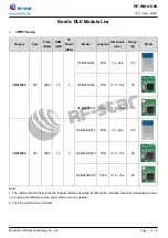
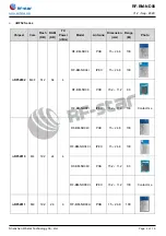
Страница 2: ...256K 16 4 RF BM ND01 PCB 15 24 8 100 RF BM ND02 PCB 13 5 16 2 80 RF BM ND02I IPEX 13 5 16 2 150 nRF51802 M0 256K 16 4 RF BM ND01C PCB 15 24 8 100 RF BM ND02C PCB 13 5 16 2 80 RF BM ND02CI IPEX 13 5 1...

Страница 3: ...n mm Range M Photo nRF52832 M4F 512 64 4 RF BM ND04 PCB 15 24 8 100 RF BM ND04I IPEX 15 24 8 100 RF BM ND08 PCB 15 2 11 2 80 RF BM ND08I IPEX 15 2 11 2 100 Contact me nRF52810 M4 192 24 4 RF BM ND04C...

Страница 4: ...D07 Chip IPEX 12 2 17 300 nRF52840 M4F 1024 256 8 RF BM ND05 PCB 15 24 8 550 RF BM ND05I IPEX 15 24 8 550 RF BM ND06 PCB 20 5 24 550 Note 1 The communication distance is the longest distance obtained...

Страница 5: ...has numerous digital peripherals and interfaces such as ADC PDM PWM I2 C and I2 S for many applications It features low power consumption small size robust connection distance and rigid reliability 1...

Страница 6: ...are of the form of RF BM ND08 where the fields are defined as follows Figure 2 Part Number Conventions of RF BM ND08 RF BM ND Company Name RF STAR Wireless Type Bluetooth Module Chipset Manufacturer...

Страница 7: ...es 7 2 Module Configuration and Functions 8 2 1 Module Parameters 8 2 2 Module Pin Diagram 9 2 3 Pin Functions 9 3 Specifications 11 3 1 Recommended Operating Conditions 11 3 2 Handling Ratings 11 3 3...

Страница 8: ...of RF BM ND08 12 Figure 5 Recommended PCB Footprint of RF BM ND08 mm 12 Figure 6 Schematic Diagram of RF BM ND08 13 Figure 7 Recommendation of Antenna Layout 14 Figure 8 Antenna Output Mode Change 15...

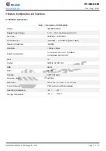
Страница 9: ...3 V Frequency 2402 MHz 2480 MHz Transmit Power 20 0 dBm 4 0 dBm Typical 0 dBm Receiving Sensitivity 96 dBm Data Rate 1 Mbps 2 Mbps Power Consumption 5 3 mA peak current in TX 0 dBm 5 4 mA peak current...

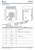
Страница 10: ...3 Pin Functions Table 2 Pin Functions of RF BM ND08 Pin Name Chip Pin Pin Type Description 1 ANT Antenna interface 2 GND GND GND Ground 3 VCC VCC VCC Power supply 1 7 V 3 6 V Recommend 3 3 V 4 P25 P0...

Страница 11: ...13 P19 P0_19 I O 14 P20 P0_20 I O 15 P05 P0_05 AIN3 I O 16 P07 P0_07 I O 17 P06 P0_06 I O 18 P08 P0_08 I O 19 P03 P0_03 AIN1 I O Note SWD debugging ports are on the bottom side of the module which is...

Страница 12: ...Operating Temperature 40 25 85 Environmental Hot Pendulum 20 20 min 3 2 Handling Ratings Table 4 Handling Ratings of RF BM ND08 Items Condition Min Typ Max Unit Storage Temperature Tstg 40 25 125 Huma...

Страница 13: ...2 Sep 2020 Shenzhen RF star Technology Co Ltd Page 12 of 19 4 Application Implementation and Layout 4 1 Module Photos Figure 4 Photos of RF BM ND08 4 2 Recommended PCB Footprint Figure 5 Recommended...

Страница 14: ...aximum value Please ensure the stable power supply and no frequently fluctuated voltage 3 When designing the power supply circuit for the module it is recommended to reserve more than 30 of the margin...

Страница 15: ...ces whose TTL protocol is the same 2 4 GHz physical layer for example USB 3 0 9 The antenna installation structure has a great influence on the module performance It is necessary to ensure the antenna...

Страница 16: ...test results by seaside are poor 3 The signal attenuation will be very obvious if there is a metal near the antenna or the module is placed inside of the metal shell 4 The incorrect power register se...

Страница 17: ...consideration in product design Static may result in the degradation in performance of module even causing the failure 4 7 Soldering and Reflow Condition 1 Heating method Conventional Convection or I...

Страница 18: ...RF BM ND08 www szrfstar com V1 2 Sep 2020 Shenzhen RF star Technology Co Ltd Page 17 of 19 Figure 9 Recommended Reflow for Lead Free Solder 4 8 Optional Packaging Figure 10 Optional Packaging Mode...

Страница 19: ...Add antenna output mode change specification Add module photo Sunny Li 2020 08 12 V1 2 Add the SWD debugging ports specification Sunny Li 2020 09 22 V1 2 Add reference design Update Nordic BLE module...

Страница 20: ...GY CO LTD Shenzhen HQ Add Room 601 Block C Skyworth Building High tech Park Nanshan District Shenzhen Guangdong China Tel 86 755 3695 3756 Chengdu Branch Add No B3 03 Building No 1 Incubation Park Hig...

Отзывы: