VC7 PCB Layout Guidelines Manual
R31UH0017EU0100 Rev.1.00
Aug 4, 2022
Page 9
5. Trace Routing
Routing a PCB board with VC7 devices should follow the generic engineering practice of PCB routing rules.
Routing recommendations are summarized in the following sections.
5.1
Single-Ended Routing
■
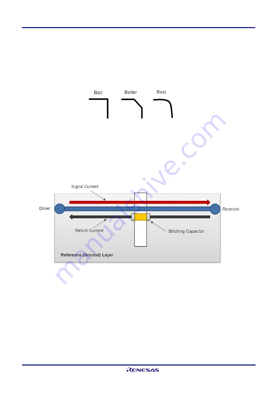
Keep clock traces as straight as possible. Use arc-shaped (or 45 degree) traces instead of right-angle or even
sharp-angle bending.
Figure 10. Trace Bending
■
Do not use multiple signal layers for clock signals (i.e., to avoid changing layers).
■
Do not use vias in clock transmission lines (i.e., to avoid changing layers). Vias can cause impedance
mismatch impairing signal integrity.
■
Always route clock signals (and any signal in that matter) on a layer that has an immediately adjacent ground
layer as a return current path.
■
As a classic routing pitfall, avoid routing a signal across a cut-out/slit on the reference plane. If unavoidable,
use a stitching capacitor (i.e., 0.1uF) to provide a return current path as follows.
Figure 11. Using a Stitching Capacitor Where Passing a Ground Plane Slit
5.2
Differential (Clock) Pair Routing
Differential traces should always be routed together (side-by-side). This keeps any noise injection into the signal
pair a true common-mode noise which gets rejected by the receiver. In a real PCB routing, consider the following
points as additional recommendations.


