VC7 PCB Layout Guidelines Manual
R31UH0017EU0100 Rev.1.00
Aug 4, 2022
Page 3
It is worth noting that stripline signals are in between two GND plane layers. This minimizes crosstalk between
the stripline signals and signals outside this layer. This is why an optimal stack-up design will enhance EMC
performance of a PCB design.
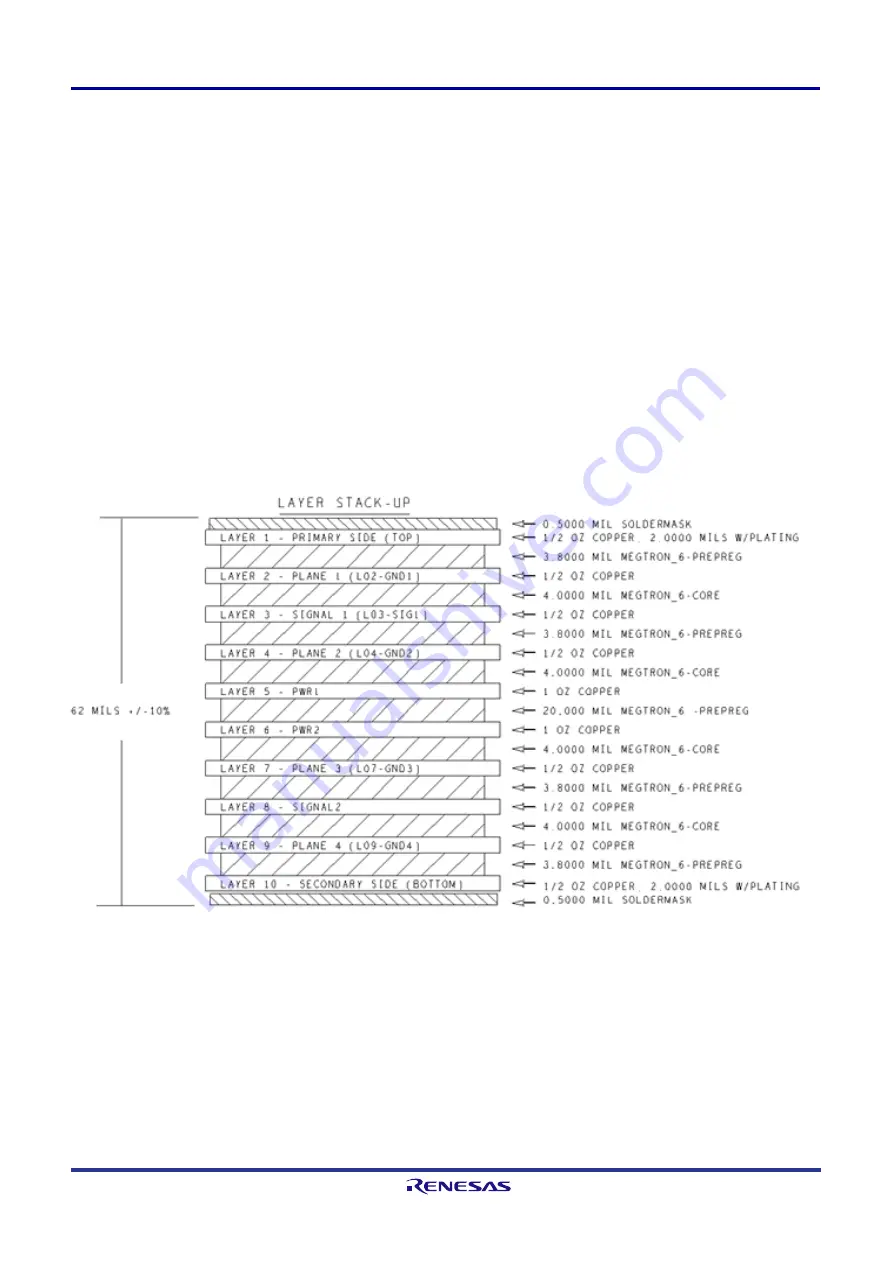
Layer stack-up is a universal requirement for any PCB design, not just for VC7 devices. The following stack-up
example is a board stack-up used for our VC7 Evaluation Board. The following comments are specific to this
board layer stack-up:
■
A 10-layer board is planned
■
6 layers are dedicated to copper planes – 4 ground planes and 2 power planes. This generous number of
ground and power planes will help the board’s EMC performance.
Note
: Depending on signal density, not every PCB board can dedicate such an abundant number of copper
planes.
■
Every signal layer must have an adjacent copper plane layer (ground or power plane) as return current paths
for the signals on that layer.
■
Megtron-6 material of different thickness are chosen as the dielectric layers between copper layers. Megtron-6
material demonstrates a very low loss at signal frequency < 2GHz. Given the clock frequencies in VC7
devices, FR4 material should be adequate.
■
Total board thinness is 62mil, which is the most common board thickness.
Figure 3. VC7 EVB Layer Stack-Up
[2]
■
From the above stack-up, Layer 3 (signal layer) is sandwiched between Layer 2 (GND plane) and Layer 4
(GND plane). Thus, Layer 3 is the preferred layer to route critical signals as noise and cross-talks are
minimalized. This is also true for Layer 8.
■
Copper layer thickness is defined by weight of copper (e.g., ½ oz of copper, or 1oz of copper). The thickness
of copper layer of 1oz is the thickness of copper when 1oz of copper is spread evenly across a square foot,
which is 0.35mm or 350mil (see the following figure).


