LTE-A Module Series
EG12 Hardware Design
EG12_Hardware_Design 58 / 97
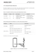
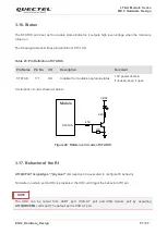
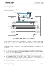
In addition, RI behavior can be configured flexibly. The default behavior of the RI is shown as below.
Table 24: Behavior of the RI
State
Response
Idle
RI keeps at high level
URC
RI outputs 120ms low pulse when a new URC returns
The RI behavior can be changed by executing
AT+QCFG="urc/ri/ring"
command. Please refer to
document [2]
for more details.
3.18. PCIe Interface*
EG12 provides one integrated PCIe (Peripheral Component Interconnect Express) interface which
complies with the PCI Express Specification, Revision 2.1 and supports 5Gbps per lane. The PCIe
interface of EG12 is only used for data transmission.
PCI Express Specification Revision 2.1 compliance
Data rate at 5Gbps per lane
Can be used to connect to an external Ethernet IC (MAC and PHY) or WLAN IC
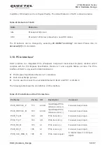
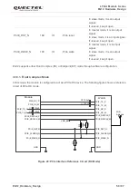
The following table shows the pin definition of PCIe interface.
Table 25: Pin Definition of the PCIe Interface
Pin Name
Pin No.
I/O
Description
Comment
PCIE_REF CLK_P
179
AI/AO
Input/Output PCIe
reference clock (+)
If unused, keep it open.
PCIE_REF CLK_M
180
AI/AO
Input/Output PCIe
reference clock (-)
If unused, keep it open.
PCIE_TX_M
182
AO
PCIe transmit (-)
If unused, keep it open.
PCIE_TX_P
183
AO
PCIe transmit (+)
If unused, keep it open.
PCIE_RX_M
185
AI
PCIe receive (-)
If unused, keep it open.
PCIE_RX_P
186
AI
PCIe receive (+)
If unused, keep it open.
PCIE_CLK_REQ_N
188
IO
PCIe clock request
In master mode, it is an input
signal.


