


LTE Module Series
EC21 Hardware Design
EC21_Hardware_Design Confidential / Released 46 / 94
PCM_CLK
PCM_SYNC
PCM_OUT
MSB
LSB
MSB
125us
1
2
256
255
PCM_IN
MSB
LSB
MSB
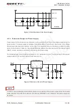
Figure 22: Primary Mode Timing
PCM_CLK
PCM_SYNC
PCM_OUT
MSB
LSB
PCM_IN
125us
MSB
1
2
16
15
LSB
Figure 23: Auxiliary Mode Timing
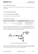
The following table shows the pin definition of PCM and I2C interfaces which can be applied on audio
codec design.
Table 14: Pin Definition of PCM and I2C Interfaces
Pin Name
Pin No.
I/O
Description
Comment
PCM_IN
24
DI
PCM data input
1.8V power domain
PCM_OUT
25
DO
PCM data output
1.8V power domain
PCM_SYNC
26
IO
PCM data frame sync signal
1.8V power domain
Quectel
Confidential


