


LTE Module Series
EC21 Hardware Design
EC21_Hardware_Design Confidential / Released 20 / 94
VDD_EXT
7
PO
Provide 1.8V for
external circuit
Vnorm=1.8V
I
O
max=50mA
Power supply for
external GPIO’s pull up
circuits.
GND
8, 9, 19,
22, 36, 46,
48, 50~54,
56, 72,
85~112
Ground
Turn on/off
Pin Name
Pin No.
I/O
Description
DC Characteristics
Comment
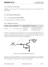
PWRKEY
21
DI
Turn on/off the
module
V
IH
max=2.1V
V
IH
min=1.3V
V
IL
max=0.5V
The output voltage is
0.8V because of the
diode drop in the
Qualcomm chipset.
RESET_N
20
DI
Reset the module
V
IH
max=2.1V
V
IH
min=1.3V
V
IL
max=0.5V
Status Indication
Pin Name
Pin No.
I/O
Description
DC Characteristics
Comment
STATUS
61
OD
Indicate the module
operating status
The drive current
should be less than
0.9mA.
Require external
pull-up. If unused,
keep it open.
NET_MODE 5
DO
Indicate the module
network registration
mode
V
OH
min=1.35V
V
OL
max=0.45V
1.8V power domain.
Cannot be pulled up
before startup.
If unused, keep it open.
NET_
STATUS
6
DO
Indicate the module
network activity
status
V
OH
min=1.35V
V
OL
max=0.45V
1.8V power domain.
If unused, keep it open.
USB Interface
Pin Name
Pin No.
I/O
Description
DC Characteristics
Comment
USB_VBUS
71
PI
USB detection
Vnorm=5.0V
USB_DP
69
IO
USB differential data
bus
Compliant with USB
2.0 standard
specification.
Require differential
impedance of 90 ohm.
USB_DM
70
IO
USB differential data
bus
Compliant with USB
2.0 standard
specification.
Require differential
impedance of 90 ohm.
Quectel
Confidential


