background image


5G Module Series 

      5G EVB User Guide 


5G_EVB_User_Guide                                                                                                                                    12 / 36 


RESET 

S0201 

Reset button (push button) 

Used to reset the module 

USB 

J1101 

USB Type C interface 

PCIe to USB 

J1601 

PCIe to USB interface, not support by default   

PCIe Configuration 

Switch 

S1501 

Used  to  configure  the  module  communication  with 

different devices via PCIe signals 

Audio 

J0802 

Codec board connector 

J0801 

Designed for loudspeakers 

J0901 

Audio jack for earphone 

(U)SIM 

J1401 

(U)SIM1 card connector 

J1402 

(U)SIM2 card connector 

SD CARD 

J1301 

SD card connector 

DBG UART 

J2002 

Debug UART port 

MAIN UART 

J2003 

Main UART port 

Status Indicator 

D0201 

Power  supply  on/off  indicator,  indicating  whether  the 
module’s power supply is on or off. 

D0202 

Module  operation  status  indicator,  indicating  whether 

the module is powered on. 

D0203 

Net  mode  indicator,  indicating  NET_MODE  status  of 

the module. 

D0204 

Net status indicator, indicating NET_STATUS status of 

the module. 

D0205 

Sleep  status  indicator,  indicating  SLEEP  status  of  the 

module. 

TE-A Connectors 

J0101, J0102 

Connectors of module TE-A 

J0802 

Connector of codec TE-A 

J1901, J1902 

Connectors of PHY TE-A 

J0701, J0702 

Connectors of Wi-Fi TE-A 

J2101, J2102 

Connectors of AP TE-A 

Antenna 

J2302,  J2305,  J2313, 

J2310,  J2316,  J2319, 

J2309,  J2306,  J2320, 

J2314, J2322, J2324 

Antenna connectors 

Содержание 5G Module Series

Страница 1: ...5G EVB User Guide 5G LTE A Module Series Rev 5G_EVB_User_Guide_V1 1 Date 2020 05 27 Status Released www quectel com...

Страница 2: ...ORMATION PROVIDED IS BASED UPON CUSTOMERS REQUIREMENTS QUECTEL MAKES EVERY EFFORT TO ENSURE THE QUALITY OF THE INFORMATION IT MAKES AVAILABLE QUECTEL DOES NOT MAKE ANY WARRANTY AS TO THE INFORMATION C...

Страница 3: ...ser Guide 5G_EVB_User_Guide 2 36 About the Document Revision History Version Date Author Description 1 0 2020 05 25 Iverson CHENG Initial 1 1 2020 05 27 Iverson CHENG Updated the firmware upgrade tool...

Страница 4: ...3 5 1 Digital Audio Codec Board Connector J0802 20 3 5 2 Analog Audio Interfaces J0901 J0801 21 3 5 2 1 Loudspeaker Interface J0801 21 3 5 2 2 Earphone Interface J0901 21 3 6 U SIM Card Interfaces J14...

Страница 5: ...5G Module Series 5G EVB User Guide 5G_EVB_User_Guide 4 36 5 Appendix A References 35...

Страница 6: ...of 5G EVB 11 Table 3 Accessories List 15 Table 4 Pin Definition of J0901 22 Table 5 Pin Definition of J1401 24 Table 6 PCIe Connection Truth Table 27 Table 7 Description of Switches and Buttons 28 Ta...

Страница 7: ...Design for Earphone Interface J0901 21 Figure 13 Pin Assignment of J0901 22 Figure 14 Schematic of Audio Plug 22 Figure 15 Simplified Connector Schematic for U SIM Card Connectors 23 Figure 16 Pin Ass...

Страница 8: ...bout usage of the EVB Evaluation Board of Quectel 5G modules The EVB is an auxiliary tool for engineers to develop and test these modules 1 1 Applicable Modules Quectel 5G EVB is applicable to the fol...

Страница 9: ...airline staff for more restrictions on the use of wireless devices on an aircraft Wireless devices may cause interference on sensitive medical equipment so please be aware of the restrictions on the...

Страница 10: ...ectel 5G and LTE A EG512R EA modules PHY TE A Interface Support PHY AR8035 AP TE A Interface Reserved SD Card Interface Support SD card U SIM Card Interface Support dual U SIM card 2 95 V and 1 8 V Au...

Страница 11: ...Pin J 0802 60 Pin CODEC TE A J 0302 J 0803 J 0805 J0301 J0402 GND RX TX J 2001 AP _ UART J1001 High Low D 0 201 POWER D 0 20 2 STATUS D0 20 3 NET _ MODE D 0 20 4 NET _ STATUS D 0 20 5 SLEEP 60 Pin J...

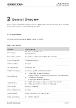
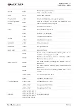
Страница 12: ...Figure 2 Bottom View for Component Placement of the EVB Table 2 Interfaces of 5G EVB Interface Reference No Description Power Supply J0303 The power jack on the EVB Typical supply voltage 5 V 3 A Powe...

Страница 13: ...Debug UART port MAIN UART J2003 Main UART port Status Indicator D0201 Power supply on off indicator indicating whether the module s power supply is on or off D0202 Module operation status indicator i...

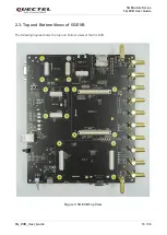
Страница 14: ...5G Module Series 5G EVB User Guide 5G_EVB_User_Guide 13 36 2 3 Top and Bottom Views of 5G EVB The following figures shows the top and bottom views of the 5G EVB Figure 3 5G EVB Top View...

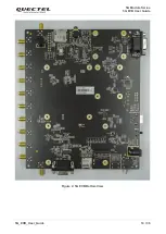
Страница 15: ...5G Module Series 5G EVB User Guide 5G_EVB_User_Guide 14 36 Figure 4 5G EVB Bottom View...

Страница 16: ...RF antennas 10 GNSS antenna passive 1 Audio Earphone 1 USB Driver Including module s related documents tools drivers etc 1 Codec TE A ALC5616 TLV320AIC3104 2 PHY TE A PHY AR8035 1 Screws Used to clam...

Страница 17: ...face USB interface Audio interfaces Digital Audio Codec Board Connector Analog Audio Interfaces Loudspeaker Interface Earphone Interface U SIM interfaces UART interfaces SD card interface PCIe to USB...

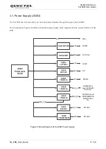
Страница 18: ...m and the power interface of 5G EVB J0303 Power Jack 5V 3A 4 2V 5V 5V Test Point Q0302 MOS U2004 TLV75533 3 3V UART U0403 MP1605 AP U0301 TPS62130 3 8V Moudle U0402 TPS62130 U0401 ISL80101 REG_3V3 SD_...

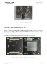
Страница 19: ...ce is designed to accommodate the TE A of the modules The TE A is mounted onto and connected to the EVB via BTB connectors J0101 and J0102 The developer will be able to test the functionalities of the...

Страница 20: ...the EVB via BTB connectors J1901 and J1902 The following two figures displays the connection between AR8035 TE A and EVB Figure 8 Connection Between AR8035 TE A and the EVB 3 4 USB Interface J1101 A...

Страница 21: ...ector J0802 The 5G EVB supports two different kinds of external digital audio codec TE As named ALC5616 and TLV320AIC3104 The codec circuit is assembled on an independent small board which can be inte...

Страница 22: ...J0801 TLV3104 LM4871 BTB CON J0802 U0801 Figure 11 Reference Circuit Design for Loudspeaker Interface J0801 3 5 2 2 Earphone Interface J0901 Audio interface J0901 is designed for earphone A reference...

Страница 23: ...J0901 Table 4 Pin Definition of J0901 The following figure shows a schematic of audio plug which suits the audio jack on 5G EVB 2 1 MIC GND SW SPK_R SPK_L 3 4 32 32 Figure 14 Schematic of Audio Plug...

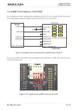
Страница 24: ...J1402 U SIM card connector USIM_VDD USIM_CLK USIM_DATA USIM_RST Module J1401 J1402 C1 C5 C6 C2 Push Push USIM_VDD USIM_DATA USIM_RST USIM_CLK USIM_PRESENCE GND USIM_PRESENCE C3 C7 C4 C8 CD GND VPP RES...

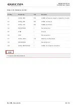
Страница 25: ...Name I O Function C1 USIM_VDD PO U SIM card power supply provided by module C2 USIM_RST DO U SIM card reset C3 USIM_CLK DO U SIM card clock C4 RESERVED Not connected C5 GND Ground C6 VPP Not connecte...

Страница 26: ...mers can easily enhance the memory capacity of modules The following figure shows the simplified interface schematic for J1301 SD Card Connector DAT2 CMD CD DAT3 VDD Module J1301 SD1_DATA2 SD1_DATA3 S...

Страница 27: ...ure shows a block diagram of UART interfaces of the EVB J0101 Module Main UART J2003 1 8V U2001 RS232 Transceiver 3 3V 1 8V Level Shift Debug UART J2002 RS232 U2002 1 8V RS232 Transceiver U2003 3 3V 1...

Страница 28: ...PCIe Connection Truth Table 3 10 Switches and Buttons S0301 S1501 S0201 S0202 The 5G EVB includes two switches S0301 and S1501 and two buttons S0201 and S0202 as shown in the following figures Figure...

Страница 29: ...ttons Table 7 Description of Switches and Buttons Interface Reference No Description Power Switch S0301 VBAT ON OFF control PWRKEY S0202 Power key used to turn on off the module PCIe Configuration S15...

Страница 30: ...ors Figure 24 Status Indicator Table 8 Description of Status Indication LEDs Reference No Description D0201 Indicates whether the power supply for module is ready On VBAT ON Off VBAT OFF D0202 Indicat...

Страница 31: ...nection between FG50V TE A and EVB J0701 FG50V TE A PCM BT_UART COEX_UART GND WLAN_EN WLAN_PWR_EN2 WLAN_PWR_EN1 VDD_1V8 BT_EN WLAN_SLEEP_CLK PCM BT_UART COEX_UART WLAN_EN WLAN_PWR_EN2 WLAN_PWR_EN1 BT_...

Страница 32: ...ies 5G EVB User Guide 5G_EVB_User_Guide 31 36 3 13 Antenna Interfaces The 5G EVB includes twelve antenna interfaces The following figure shows the assembly of these antenna interfaces Figure 27 Antenn...

Страница 33: ...Then D0201 ON OFF indicator of the module s power supply will light up 5 Press the S0202 PWRKEY for at least 500ms then the module will be powered on and D0202 operation indicator of the module will...

Страница 34: ...tting Field on QCOM USB AT Port Connection 4 3 Firmware Upgrade Firmware of the module is upgraded via USB port by default and there are two methods for the upgrade emergency download and normal downl...

Страница 35: ...dule The reset option is only used in case of abnormality For example the software fails to respond for more than 5 s due to some serious problems Long press the button S0201 RESET for more than 250 m...

Страница 36: ...guide of Windows USB drivers for Quectel LTE and 5G modules 2 Quectel_QCOM_User_Guide The user guide of QCOM 3 Quectel_QFlash_User_Guide The user guide of QFlash Abbreviation Description AGND Analog...

Страница 37: ...te Computer PCB Printed Circuit Board PCM Pulse Code Modulation PHY Physical Layer PO Power Output RF Radio Frequency SD Secure Digital SIM Subscriber Identity Module UART Universal Asynchronous Recei...

Отзывы: