background image

VFO Circuit

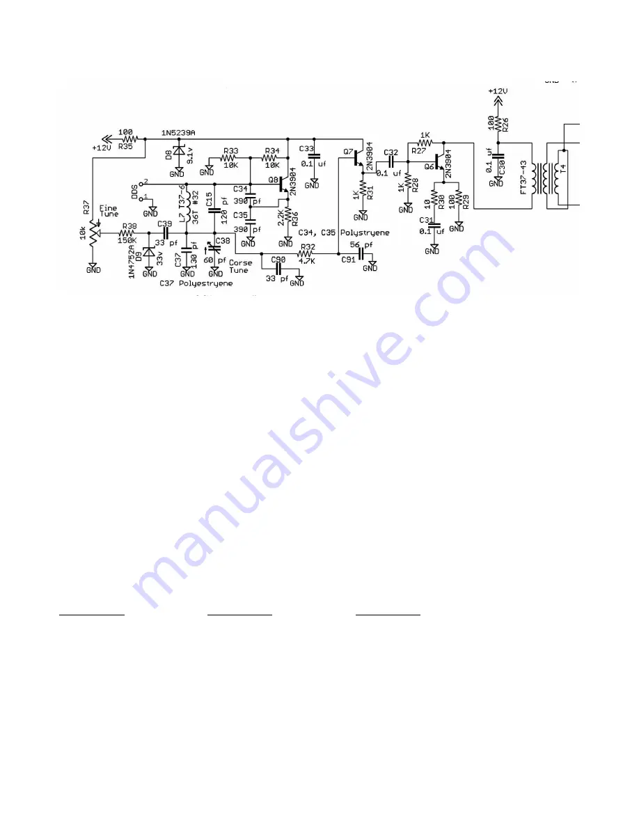
Bias for Q­7 is developed from the same two resistors (R­33 and R­34) that provide bias for Q­8.
Main frequency determining components of the VFO include L­7, C­34 & C­35, C­15, C­37, C­90, and 
C­38.  D9 acts as a voltage variable capacitor in series with C­39 to provide Fine Tuning control.   For 

adequate VFO stability C­34, C­37, and C­35 should be polystyrene types (these are semi­transparent 
plastic).  C­15, C­39, and C­90 should be NPO types (they have a black band on the top section).
For operation on 17 meters, the VFO operates 12.96 MHz below the desired frequency (18.068 – 12.96 
= 5.108 MHz and 18.168 ­12.96 = 5.208 MHz) so the VFO needs to tune over the range of 5.108 to 

5.208 MHz.  VFO alignment steps are:

1. Set the Fine Tune potentiometer to mid­point.
2. Open C­38 (the polyvaricon) to minimum capacitance.
3. Adjust C­38 trimmer capacitor so the VFO is operating at or just above 5.208 MHz.  If you 

cannot reach that frequency, try changing the values of C­90, then C­37, and lastly C­15.

4. Close C­38 (the polyvaricon) to maximum capacitance and verify that your VFO frequency is 

now below 5.108 MHz.

Waveforms present in this oscillator will affect the accuracy of DC voltmeters.  In order to measure 

these potentials you should stop the oscillator by temporarily connecting a 0.1 mfd capacitor across 
R­36.

Q­8 Voltages

Q­7 Voltages

Q­6 Voltages

Collector  9.13 VDC

Collector  9.13 VDC

Collector    7.98 VDC

Emitter     3.75 VDC

Emitter     3.64 VDC

Emitter       3.16 VDC

Base      4.40 VDC

Base      4.29 VDC

Base        3.88 VDC

(Remember to remove the 0.1 that was installed to stop the oscillator)

Page 29 of 34

Содержание BITX20A

Страница 1: ...the BITX17A design The basic design for both 20 meters and 17 meters is the same thus DC voltages and troubleshooting methods remain the same except for obvious frequency differences There is a BITX...

Страница 2: ...t components in their place Some care is required to avoid damaging the PCB in the un soldering and re soldering process Solder wick or a section of braid salvaged from a length of coaxial cable shiel...

Страница 3: ...100 pf Ceramic Capacitor C 47B 82 pf 100 pf Ceramic Capacitor C 48A 150 pf 180 pf Ceramic Capacitor C 48B 150 pf 180 pf Ceramic Capacitor C 49A 82 pf 100 pf Ceramic Capacitor C 49B 82 pf 100 pf Cerami...

Страница 4: ...Parts Placement Diagram Drawing by KD1JV Page 4 of 34...

Страница 5: ...BITX17A Schematic Diagram Drawing by N7VE Page 5 of 34...

Страница 6: ...TE Before you install the new crystal for X 5 you may want to temporarily insert each new 12 96 MHz crystal into the BFO oscillator position X 5 and measure the default frequency for each crystal meas...

Страница 7: ...92 51 pf Ceramic Capacitor Remove C 54 82 pf Ceramic Capacitor Install new C 54 68 pf Ceramic Capacitor Remove C 55 100 pf Ceramic Capacitor Install new C 55 82 pf Ceramic Capacitor Remove C 56 100 pf...

Страница 8: ...move C 35 470 pf Polystyrene Capacitor Install new C 35 390 pf Polystyrene Capacitor Remove C 37 220 pf Polystyrene Capacitor Install new C 37 130 Polystyrene Capacitor Clip excess lead length Inspect...

Страница 9: ...7 VFO Oscillator Coil Remove 14 turns This should leave 36 turns on the core Re install L 7 Remove L 6 RF Filter Coil Remove 4 turns This should leave 14 turns on the core Re install L 6 Remove L 4 R...

Страница 10: ...e the 0 to 300 ma levels using voltage across a resistor This will be discussed in the alignment procedures The Microphone that you are going to use with this transceiver or an audio signal generator...

Страница 11: ...lly adjust C 14 and C 18 for maximum received signal level There is some interaction between these 2 capacitors so you may need to re peak each capacitor adjustment several times to reach maximum sens...

Страница 12: ...d Aaaaaaaaaaah into the microphone will also work if you do not have an audio signal generator Key the transmitter and slowly rotate R 83 to the right while watching the transmitter RF output An RMS v...

Страница 13: ...Parts Placement Drawing Drawing by KD1JV Page 13 of 34...

Страница 14: ...Schematic Diagram Schematic by N7VE Page 14 of 34...

Страница 15: ...n key the transmitter Key the transmitter again and adjust the BFO Carrier Oscillator frequency C 72 for maximum signal level note the frequency on the counter and then adjust C 72 for a lower frequen...

Страница 16: ...citor will provide some adjustment but you will need to select which capacitor sections are connected to set the minimum maximum tuning limits and the tuning range Polyvaricon Capacitance Trimmer Open...

Страница 17: ...ed in adjusting the transmitter drivers section but you do have to set the bias adjustment Drive level adjustment will be done in the RF PA alignment section 1 Connect a 2 to 3 ampere DC ammeter in se...

Страница 18: ...ld set the RF output level no higher than the point where RF compression becomes apparent As you monitor the RF output and simultaneously increase the drive level you should see the output rise fairly...

Страница 19: ...The following voltage measurements are made in receive mode LM386 Voltages Q 16Voltages Q 25 Voltages Pin 1 1 34 VDC Collector 10 97 VDC Collector 5 94 VDC Pin 2 0 0 VDC Emitter 5 26 VDC Emitter 0 0...

Страница 20: ...common in inexpensive audio devices tape recorders etc or can be purchased directly from component suppliers Most inexpensive computer microphones are Electret types Audio input level for transmitter...

Страница 21: ...VXO adjustment allows you to set the crystal oscillator to it s proper frequency which is 12 to 20 db down the lower sideband skirt of the crystal filter Because the oscillating waveform will affect...

Страница 22: ...minimum output There should be two points on C 65 where the R 64 voltage is at minimum this verifies that you are not at the end of the adjustment range The dip in voltage across R 64 should occur at...

Страница 23: ...ly across the IF passband note and record R 64 signal levels at every 200 Hz frequency step For a rather crude looking chart you can simply plot the voltage readings on graph paper to determine your f...

Страница 24: ...bandwidth The value of C 55 should equal approximately twice the value of C 54 or C 56 but there is some room to experiment to see how changes affect the ripple factor across the passband and steepne...

Страница 25: ...Receive 1st IF Amplifier Q 9 Voltages voltage measurements are made in receive mode Collector 7 62 VDC Emitter 1 62 VDC Base 2 35 VDC Page 25 of 34...

Страница 26: ...d Q 17 providing current gain Overall amplification is controlled by feedback divider made up of R 52 and R 55 Q 11 voltages Q 17 voltages voltage measurements are made in receive mode Collector 4 61...

Страница 27: ...Transmit 1st IF Amplifier Q 12 Voltages measured in transmit mode Collector 8 57 VDC Emitter 1 93 VDC Base 2 65 VDC Page 27 of 34...

Страница 28: ...Transmit 2nd IF Amplifier Q 10 Voltages measured in transmit mode Collector 7 59 VDC Emitter 1 63 VDC Base 2 35 VDC Page 28 of 34...

Страница 29: ...alignment steps are 1 Set the Fine Tune potentiometer to mid point 2 Open C 38 the polyvaricon to minimum capacitance 3 Adjust C 38 trimmer capacitor so the VFO is operating at or just above 5 208 MHz...

Страница 30: ...Receive RF Amplifier Q 5 Voltages measured in receive mode Collector 7 62 VDC Emitter 1 65 VDC Base 2 36 VDC Page 30 of 34...

Страница 31: ...68 and L 10 form a series resonant bandpass filter to block VFO and IF energy from reaching the transmit amplifier stages Q 4 Voltages measure in transmit mode Collector 7 60 VDC Emitter 1 61 VDC Base...

Страница 32: ...and L 4 will not tune to midpoint in the 17 meter band adjustment should be made by adding or subtracting turns on L4 If C 20 C 18 and L 6 will not tune to midpoint in the 17 meter band adjustment sho...

Страница 33: ...ing transmit and shunts RF to ground during that period Q 26 2N7000 is in OFF mode during transmit and blocks RF during transmit Q 24 2N7000 is in ON mode during transmit and shunts RF to ground durin...

Страница 34: ...VDC Emitter 2 52 VDC Base 3 27 VDC Q 18 BS170 Q 19 BS170 Drain 11 46 VDC Drain 11 46 VDC Source 0 044 VDC Source 0 044 VDC Gate adjust VDC Gate adjust VDC 20 ma 0 044 volts DC Q 1 IRF510 Q 2 IRF510 D...

Отзывы: