QRPGuys Digital DSB II Transceiver Kit Скачать руководство пользователя страница 6

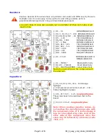
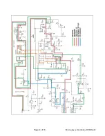
Page 6 of 16                                      ft8_II_assy_smd_diode_072020.pdf 

Everything else:


[ ] U3 – 7809 Bend the leads at the point 
where they narrow. Secure with 4-40 screw 
and nut.  
[ ] J5, J6, J7 – 5 pins SIP socket. Make sure 
these are set square to the board before 
soldering more than one pin.  
 
 
[ ] U2 - 8 pin DIP socket. Note orientation of 
notch on socket and match with notch on part 
board outline. Make sure all the pins are 
sticking out the solder pads before soldering 
any! 
[ ] J3, J4 – 3.5mm phone jacks 
[ ] Q1, Q2, Q4 – BS170 MOSFET Note 
orientation of the flat side of part. Make sure it 
matches the board outline.  
[ ] Q3, Q9 – 2N3904 NPN 
[ ] Q5 – 2N3906 PNP 

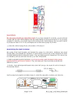
[ ] Q6, Q7, Q8 – These parts require some heat sinking. Therefore, these parts get mounted with 
the flat side of the package pressed against the large, tinned pad to the left of the board. Make 
“U” shaped pieces of resistor lead clippings to hold the body of  the BS170's to the board, using 
the small holes on either side of the package. 


[ ] D4 – CLEAR LENS RED LED – the 

short

 lead goes into hole on flat side of part outline. 

[ ] TEST – 2 pin SIP header, short pin end in the board 
[ ] V1, V2 – 2K trimmer pots 
[ ] J2 – DC power Jack.  
[ ] J1 – BNC antenna jack 


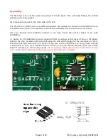
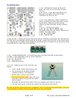
[ ] T1, T2 – bifilar wound on T37-43 ferrite core 
(black).  


Cut 6” length of each color magnet wire 


The two wires can be lightly twisted 
together, but this is not necessary 


Wind 5 turns on the core as shown. 


Trim and tin the wire ends

.

 Either scrape or 

melt the insulation using a hot iron with a 
blob of solder. 


Orientate the common wire ends so they are opposite each other on the core. 


The wires will now be in the proper position for inserting into the board. 

Be sure to tin the wire ends before installing. This is a leading cause of failure. Be sure 
not to pull the wire thru the hole past where you have it tinned. 

Содержание Digital DSB II Transceiver Kit

Страница 1: ...ts List Location Quantity value Type C1 C2 C10 C13 C16 5 10 nF 103 X7R MMLC C3 C7 2 100 uF electrolytic 16V Long lead plus C4 C5 C6 C8 C9 C12 C14 C15 C18 C19 C20 C22 12 100 nF 104 X7R MMLC C11 C17 C21...

Страница 2: ...MEG BRN BLK GRN GLD U1 1 SA602 or SA612A SO8 MIXER OSC U2 1 LM358 DIP8 DUAL OPAMP U3 1 LM7809 TO 220 9V 1A REG V1 V2 2 2K 6mm Trimmer resistor T1 T2 2 FT37 43 FERITE CORE BLACK DIP SOCKET 1 8 PIN DIP...

Страница 3: ...2 uH RED RED GLD GLD or RED RED GLD SIL 4 T37 2 RED CORES 2 T37 6 YELLOW CORES crystals 1 7 074 MHz HC 49 US 1 10 136 MHz HC 49 US 1 14 074 MHz HC 49 US Miscellaneous 3 Band module boards 12 1 26 magn...

Страница 4: ...ite smd soldering method or we have found the process below to be quite satisfactory Solder U1 the SA602 612 smd component first by wiping a thin layer of flux on the board position the chip carefully...

Страница 5: ...1 R20 5 6 GRN BLU GLD GLD R13 470K YEL VOL YEL GLD R14 47K YEL VOL ORG GLD R15 680K BLU GRY YEL GLD L4 10 uH BRN BLK BLK GLD or BRN BLK BLK SIL D1 1N5817 Black plastic body D2 D3 1N4148 Small Glass bo...

Страница 6: ...t of the board Make U shaped pieces of resistor lead clippings to hold the body of the BS170 s to the board using the small holes on either side of the package D4 CLEAR LENS RED LED the short lead goe...

Страница 7: ...three band modules and detailed the values for 20 30 40m Additional bare band module pcb s are available for operation on other bands At the end of this document we have modeled additional band compo...

Страница 8: ...L2 20 turns on T37 2 RED core make sure turns are snug to the core and more or less evenly spaced around the core Loose winding does not work well L3 18 turns on T37 2 RED core X1 7 074 MHz crystal I...

Страница 9: ...top of the board centered on the silkscreen outline Secure each toroid to the pcb using two of the supplied plastic zip ties as shown below Be sure to tin the wire ends before installing The transceiv...

Страница 10: ...card output level until the board switches into Transmit RED LED goes on you can continue to increase the output level a little bit to ensure reliable triggering of the VOX circuit If you have a watt...

Страница 11: ...card to the mixer input This allows you to set the audio output from the sound card to a reasonable level and not overdrive the mixer The other half of the LM358 U2a is used as a VOX circuit The peak...

Страница 12: ...nd your meter Only be concerned if the voltages are significantly different than those shown Almost all of the construction issues with the DSB transceiver have been traced to the faulty installation...

Страница 13: ...Drain G Gate S Source E Emitter B Base C Collector I Input G Ground O Output Pin 1 2 3 4 5 6 7 8 U1 1 42 1 42 0 7 15 7 15 8 3 7 5 8 35 U2 Rx 0 0 0 0 4 5 4 5 4 5 9 Rx D C G B S E Tx D C G B S E Q1 0V...

Страница 14: ...Page 14 of 16 ft8_II_assy_smd_diode_072020 pdf...

Страница 15: ...Page 15 of 16 ft8_II_assy_smd_diode_072020 pdf...

Страница 16: ...___________________ _________________________________________________ _________________________________________________ _________________________________________________ ______________________________...

Отзывы: