2
3. Design
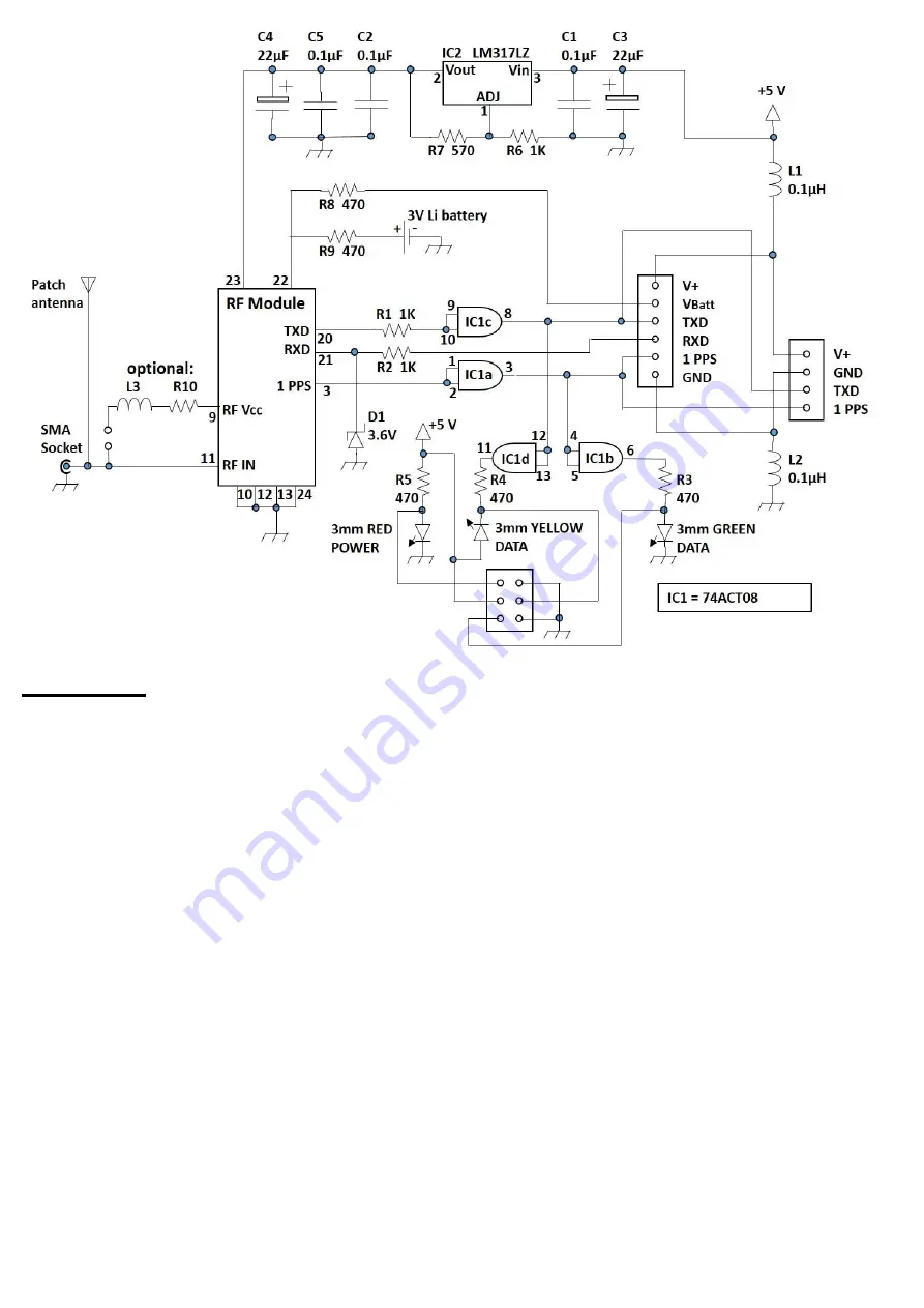
The design is quite simple. Note the circuit diagram above. The GPS receiver RF module does all the hard
work. The additional circuits are supply filtering, voltage regulation (the module requires 3.3V operation),
level shifting, and LED indication.
Supply voltage filtering is undertaken by two 0.1uH inductors in series with both the +5V and ground
supplies, and plenty of smoothing/decoupling capacitors (the 0.1uF and 22uF capacitors). The voltage
regulator is an LM317LZ configured for 3.3V output. Additionally there is a 3V Li rechargeable battery on
the board. This is charged automatically during operation. When power is removed, it retains ephemeris
information in the RF receiver module. This enables a faster fix, next time the GPS receiver is powered.
The data output and 1pps output from the RF module are at 2.8V level (via internal voltage regulation
within the module). The 74ACT logic family are perfect for the purposes of level conversion, because the
“high” voltage threshold specification for this family is below the 2.8V “high” output voltage of the RF
module. This is therefore converted to 5V by the 74ACT08 quad AND-gate, which is configured as four
buffers. The voltage to the serial data input of the RF module is restricted by zener diode D1.
The kit includes three 3mm LEDs. It is suggested to fit the Red LED to be permanently on, to show power
to the board. The Yellow and Green LEDs indicate respectively, serial data and the 1pps signal. They are
driven by the remaining two AND gates of the 74ACT08. Note that the serial data output is idle-high, i.e. at
5V in the pause between data bursts. Therefore the yellow LED is connected to 5V, so as to light when the
serial line is LOW. It will therefore pulse once per second during the data burst. The green 1pps LED will
only pulse once a GPS fix is attained
– the Green colour traditionally indicating “All is well”.


