background image


6


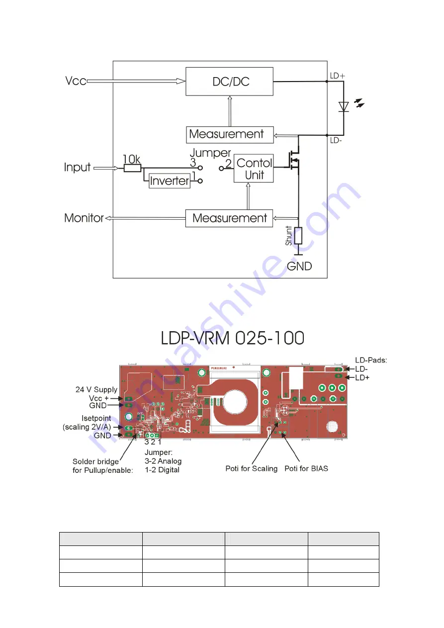
Power Driver Block Diagram 


Description of the Connectors 


Power Supply and absolute maximum Ratings 


Pin of conn. #3 

Allowed range 

Best performance 

Destroying limit 

1 VCC (laser supply) 

24 V .. 26 V 


30 V 

2 (GND) 

GND 

GND 


3 (Input terminal) 

0 V .. 5 V 

+ 5.3 V 

Содержание LDP-VRM 025-100 CA

Страница 1: ...User Manual PicoLAS GmbH Burgstr 2 52146 Würselen Germany Phone 49 0 2405 64594 60 Fax 49 0 2405 64594 61 E mail info picolas de Web www picolas de Rev 1909 LDP VRM 025 100 CA ...

Страница 2: ...t Overview 4 How to get started 5 Required Laser Diode Pinout 6 Power Driver Block Diagram 6 Description of the Connectors 6 Power Supply and absolute maximum Ratings 6 Input 7 Jumper 7 Current Monitor 7 Bias and scaling Potentiometers 7 Test Load 7 Power Dissipation 7 Mechanical Dimensions 7 ...

Страница 3: ...GND and beyond VCC VCC Limit see table in section Power Supply 3 Peak output current 2 5 A Operating temperature range 0 C 60 C Best performance operating temperature range 10 C 35 C Storage temperature range 20 C 70 C Dos and Don ts Never ground any output connector Never use any grounded probes at the output Do not connect your oscilloscope to the output Driver and the probe will immediately be ...

Страница 4: ...4 ...

Страница 5: ...er source 5 Adjust scaling and bias See potentiometer for scaling a bias 6 Feed a signal on the input terminal For example 1 kHz sine wave with 1 V amplitude Make sure not to overload the laser diode or the driver Range of input signal 0 V 5 V 7 Monitor the current output The current monitor measures a signal comparable with the input signal Use an oscilloscope with a 1 MEG ohm termination Scale 1...

Страница 6: ... Diagram Description of the Connectors Power Supply and absolute maximum Ratings Pin of conn 3 Allowed range Best performance Destroying limit 1 VCC laser supply 24 V 26 V 30 V 2 GND GND GND 3 Input terminal 0 V 5 V 5 3 V ...

Страница 7: ...ent The scaling potentiometer varies with the scaling of the input signal Turn it right to increase the scale from 0 A V to 0 5 A V Test Load For the first test an appropriate test load may be assembled instead of the laser diode This test load can either be a short circuit or a Schottky diode like the ES3C Please connect the test load only between anode and cathode LD and LD and prevent shorts to...

Отзывы: