Circuit Descriptions, List of Abbreviations, and IC Data Sheets
9.
The volume level is controlled at this IC (pin 9) by the
"VOLUME" control line coming from the microprocessor. After
amplification, the audio signal is sent to the speaker /
headphone output connector.
9.3.3
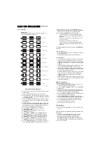
AVL (Automatic Volume Limiting)
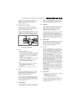
The "Mono AVL" function operates via the UOC. During
channel change and source selection, the AVL bit is to be
switched "off" and then can return to the previous state ("on/
off") as shown in the timing diagram below.
The "Stereo AVL" function operates via the AGC control of IC
TDA9853H. During channel change and source selection, the
AGC function is to be switched "off" and then can resume to the
previous state ("on/off") as shown in timing diagram below.
Figure 9-1 AVL timing diagram
9.3.4
Mute
The TV set must mute:
•
Whenever a "User Mute" is activated.
•
Whenever there is a channel change, RF to RF, RF to AV,
AV to RF, and AV to AV (if any). In channel change, MUTE
must be activated first before any other activity and un-
MUTE must be done after every other activity has been
completed.
•
Whenever there is a loss in the signal.
•
During cold or warm start, MUTE must be activated until all
initialization processes are finished.
•
When the set is going to STANDBY, MUTE must be
activated first before any other activities.
Note:
1.
MUTE mentioned above applies to the audio amplifier
mute (= PWM volume control mute).
2.
The first condition does not apply for the UOC, IC
TDA9853H.
3.
Above conditions refers to both mono and stereo sets.
9.4
Video
For a detailed circuit description of this part, we refer to the
L01.2L AA manual (see the beginning of this chapter for the
ordering codes). Please note that there can be minor
differences in the text (e.g. other item numbers), but the
described circuit principle is comparable.
This chassis uses the TDA937x family Ultimate One Chip TV
processor (UOC), which is mounted in an SDIP 64 envelope.
The various versions of the UOC series combine the function
of a video processor together with a microcontroller and US
Closed Caption/TXT decoder.
9.5
Synchronization
Inside IC7200 (part D) the vertical and horizontal sync pulses
are separated. These "H" and "V" signals are synchronized
with the incoming CVBS signal. They are then fed to the H- and
V-drive circuits and to the OSD/TXT circuit for synchronization
of the On Screen Display and Teletext (CC) information.
9.6
Deflection
For a detailed circuit description of this part, we refer to the
L01.2L AA manual (see the beginning of this chapter for the
ordering codes). Please note that there can be minor
differences in the text (e.g. other item numbers), but the
described circuit principle is comparable.
The L03 range consists of TV sets spanning from 14 to 21 inch
using the same chassis architecture. For the chassis
architecture, the CRTs used do not need East/West Correction.
Therefore the geometry correction needed is horizontal shift,
vertical slope, vertical amplitude, vertical S-correction, vertical
shift and vertical zoom for geometry corrections (with the
appropriate offsets required for NTSC channels on PAL sets).
9.7
Power Supply
For a detailed circuit description of this part, we refer to the
L01.2L AA manual (see the beginning of this chapter for the
ordering codes). Please note that there can be minor
differences in the text (e.g. other item numbers), but the
described circuit principle is comparable.
9.7.1
Introduction
The supply is a Switching Mode Power Supply (SMPS). The
frequency of operation varies with the circuit load. This 'Quasi-
Resonant Flyback' behavior has some important benefits
compared to a 'hard switching' fixed frequency Flyback
converter. The efficiency can be improved up to 90%, which
results in lower power consumption. Moreover, the supply runs
cooler and safety is enhanced.
The control IC in this power supply is the TEA1506 (L01=
TEA1507). Unlike the TEA1507 control IC, the TEA1506 has
no internal high voltage start-up source, and therefore needs to
be started by means of an external bleeder resistor (R3506 and
R3507). The operating voltage for the driver circuit is also taken
from the 'hot' side of this transformer.
The switching regulator IC 7520 starts switching the FET 'on'
and 'off', to control the current flow through the primary winding
of transformer 5520. The energy stored in the primary winding
during the 'on' time is delivered to the secondary windings
during the 'off' time.
The "MainSupply" line is the reference voltage for the power
supply. It is sampled by resistors 3543 and 3544 and fed to the
input of the regulator 7540 / 6540. This regulator drives the
feedback optocoupler 7515 to set the feedback control voltage
on pin 6 of 7520.
The power supply in the set is "on" any time AC power is
connected to the set.
9.7.2
Derived Voltages
The voltages supplied by the secondary windings of T5520 are:
•
"MainSupply" for the horizontal output.
•
"V
aux
/V
audio
" for the audio circuit.
•
An optional "DVD
Supply
" for future extensions.
Other voltages are provided by the LOT. It supplies -12 V, the
tuner voltage, the filament voltage, and the +160 V source for
the video drive. These secondary voltages of the LOT are
monitored by the "EHT" lines.
Mono: AVL_ On/Off
Stereo: AGC_On/Off
channel / source
change active
Mu te/Volume
user press
Ch+ / Ch- or
change
source
Volume Ctrl Voltage
200 msecs
150 msecs
50 msecs
50 msecs
CL 36532044_038.eps
170603
Содержание L03.2L AA
Страница 1: ......


