Circuit Description
9.
inserts the cut-off point measuring pulses into the RGB signals
during the vertical retrace period.
The following additional controls are used:
•
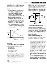
Black current calibration loop. Because of the 2-point
black current stabilization circuit, both the black level and
the amplitude of the RGB output signals depend on the
drive characteristics of the picture tube. The system checks
whether the returning measuring currents meet the
requirements, and adapt the output level and gain of the
circuit when necessary. After stabilization of the loop, the
RGB drive signals are switched on. The 2-point black level
system adapts the drive voltage for each cathode in such a
way that the two measuring currents have the right value.
This is done with the measurement pulses during the frame
flyback. During the first frame, three pulses with a current
of 8
µ
A are generated to adjust the cut off voltage. During
the second frame, three pulses with a current of 20
µ
A are
generated to adjust the 'white drive'. This has as a
consequence, that a change in the gain of the output stage
will be compensated by a gain change of the RGB control
circuit. Pin 55 (BLKIN) of the UOC is used as the feedback
input from the CRT base panel.
•
Blue stretch. This function increases the color
temperature of the bright scenes (amplitudes which
exceed a value of 80% of the nominal amplitude). This
effect is obtained by decreasing the small signal gain of the
red and green channel signals, which exceed this 80%
level.
•
Beam current limiting. A beam current limiting circuit
inside the UOC handles the contrast and brightness control
for the RGB signals. This prevents the CRT from being
overdriven, which could otherwise cause serious damage
in the line output stage. The reference used for this
purpose is the DC voltage on pin 54 (BLCIN) of the TV
processor. Contrast and brightness reduction of the RGB
output signals is therefore proportional to the voltage
present on this pin. Contrast reduction starts when the
voltage on pin 54 is lower than 2.8 V. Brightness reduction
starts when the voltage on pin 54 is less than 1.7 V. The
voltage on pin 54 is normally 3.3 V (limiter not active).
During set switch-off, the black current control circuit
generates a fixed beam current of 1 mA. This current
ensures that the picture tube capacitance is discharged.
During the switch-off period, the vertical deflection is
placed in an over-scan position, so that the discharge is not
visible on the screen.
9.3.7
RGB Amplifier
From outputs 56, 57, and 58 of IC 7200 the RGB signals are
applied to the integrated output amplifier (7330) on the CRT
panel. Via the outputs 7, 8, and 9, the picture tube cathodes are
driven.
The supply voltage for the amplifier is +200 V and is derived
from the line output stage.
9.3.8
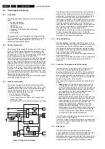
Eco Scavem (diagram B2 if present)
The SCAn VElocity Modulation (Scavem) circuitry is
implemented in the layout of the picture tube panel. It is thus
not an extra module. This circuit influences the horizontal
deflection as a function of the picture content. In an ideal
square wave, the sides are limited in slope due to a limited
bandwidth (5 MHz). Scavem will improve the slope as follows:
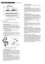
•
At a positive slope, a Scavem current is generated which
supports the deflection current. At the first half of the slope,
the spot is accelerated and the picture is darker. At the
second half of the slope, the spot is delayed and the slope
becomes steeper.
•
At the end of the slope, the Scavem-current decays to
zero and the spot is at the original position. An overshoot
occurs which improves the impression of sharpness.
•
At the negative slope, the Scavem-current counteracts
the deflection. During the first half of the slope, the spot is
delayed and the slope becomes steeper. During the
second half the spot accelerates, the Scavem-current is
zero at the end of the slope.
The RGB signals are fed into the Scavem circuit and
differentiated by C2364/2365/2366 and the input impedance of
the TS7360 stage. Diode D6364 (Schottky diode) is the coring
component, which blocks all the signals below 0.3 V so that the
noise is not amplified and all the signals larger than 0.3 V are
differentiated and amplified.
After differentiation, the signal is amplified by TS7360 with
R3369 as the collector resistor. The biasing of the TS7360
stage is done by R3369, R3361, R3360, R3362, and R3363.
Items D6367, C2367, R3367, R3361, and C2360 work as the
clipping components that limit the Scavem current at a certain
level, to prevent Scavem over-correction.
After being buffered by TS7369, the differentiated signals are
coupled through C2375 and C2380 to the output stage. The
output stage is configured into cascode stage and push-pull
operation. The biasing is done by R3373, R3375, R3376,
R3380, R3381, R3383, R3374, and R3384. The working
voltage of the transistors is settled at half the supply voltage.
At the rising portion of the RGB signals, cascode TS7380 and
TS7382 will be operating and will pull the current through the
Scavem coil. Contrarily, at the falling portion of the RGB
signals, cascode TS7373 and TS7366 will be operating and will
push the current through the Scavem coil.
The capacitors C2362, C2373, and C2381 ground the high
frequencies, to prevent high frequency amplification. The ferrite
bead L5376 is for EMC purpose. Resistors R3374 and R3384
determine the output Scavem current.
Items C2378 and R3378 are for the fine-tuning for different
Scavem coil impedances. They also help to suppress high
frequency oscillation. Capacitor C2369 helps to suppress the
high frequency components and controls the Scavem delay.
9.4
Synchronization
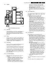
Inside IC 7200 part D, the vertical and horizontal sync pulses
are separated. These 'H' and 'V' signals are synchronized with
the incoming CVBS signal. They are then fed to the H- and V-
drive circuits and to the OSD/TXT circuit for synchronization of
the On Screen Display and Teletext (CC) information.
9.5
Deflection
Please use the diagrams in chapter 6 and/or 7 for elucidation
of the descriptions below.
9.5.1
Horizontal Drive
The horizontal drive signal is obtained from an internal VCO,
which is running at twice the line frequency. This frequency is
divided by two, to lock the first control loop to the incoming
signal.
When the IC is switched 'on', the 'Hdrive' signal is suppressed
until the frequency is correct.
The 'Hdrive' signal is available at pin 30. The 'Hflybk' signal is
fed to pin 31 to phase lock the horizontal oscillator, so that
TS7462 cannot switch 'on' during the flyback time.
The 'EWdrive' signal for the E/W circuit (if present) is available
on pin 15, where it drives transistor TS7400 to make linearity
corrections in the horizontal drive.
When the set is switched on, the '+8V' voltage goes to pin 9 of
IC7200. The horizontal drive starts up in a soft start mode. It
starts with a very short T_on time of the horizontal output
transistor. The T_off of the transistor is identical to the time in
normal operation. The starting frequency during switch on is
Содержание L01.1L AC
Страница 6: ...Directions for Use EN 6 L01 1L AC 3 3 Directions for Use 3 1 16 9 Sets ...
Страница 7: ...Directions for Use EN 7 L01 1L AC 3 ...
Страница 8: ...Directions for Use EN 8 L01 1L AC 3 ...
Страница 9: ...Directions for Use EN 9 L01 1L AC 3 ...
Страница 10: ...Directions for Use EN 10 L01 1L AC 3 ...
Страница 11: ...Directions for Use EN 11 L01 1L AC 3 ...
Страница 12: ...Directions for Use EN 12 L01 1L AC 3 ...
Страница 13: ...Directions for Use EN 13 L01 1L AC 3 ...
Страница 14: ...Directions for Use EN 14 L01 1L AC 3 ...
Страница 15: ...Directions for Use EN 15 L01 1L AC 3 ...
Страница 16: ...Directions for Use EN 16 L01 1L AC 3 Personal Notes ...
Страница 17: ...Directions for Use EN 17 L01 1L AC 3 3 2 4 3 Sets Personal Notes ...
Страница 42: ...Spare Parts List EN 82 L01 1L AC 10 10 Spare Parts List Not applicable yet ...
Страница 43: ...Revision List EN 83 L01 1L AC 11 11 Revision List First release ...

