


Service Modes, Error Codes, and Fault Finding
EN 25
BJ2.4U/BJ2.5U LA
5.
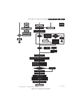
Figure 5-10 “Semi Stand-by” to “Active” 32” LCD LPL Scanning Backlight flowchart
G_15910_009.eps
230606
32" LCD LPL scanning backlight
Switch on 12V LCD supply
(LCD-Power-on)
Start to apply valid interface signals to the module (LVDS) within a
time frame of min. 17.5ms to max. 67.5ms after supply switch on.
In implementation, use 25ms, this makes it compatible with 32"Sharp
(t=17.5ms is the supply switch-on delay taken into account)
Active
Semi Standby
action holder: MIPS
autonomous action
action holder: St-by
Switch off RGB blanking
Initialize audio and video processing IC's and
functions according needed use case.
Assert RGB video blanking
and audio mute
Wait until previous on-state is left more than
2
seconds
ago. (to prevent LCD display problems)
The assumption here is that a fast
toggle (<2s) can only happen during ON-
>SEM I ->ON. In these states, the Viper is
still active and can provide the 2s delay.
If the transition ON->SEM I->STBY->SEM I-
>ON can be made in less than 2s, we
have to delay the semi -> stby transition
until the requirement is met.
Switch Audio-Reset and sound enable low and demute
(see CHS audio LdspMute interface).
Wait until QVCP generates a valid lvds output
clock.
Switch on LCD lamp after valid, stable video, corresponding
to the requested output is delivered by the Viper
Switch off backlight (FMS scan rate conversion interface) to
prevent backlight to freerun after preheating phase.
Set scanning backlight to Normal scanning using the
FMS scan rate conversion interface.
Содержание 37-LCD 37PF9431D
Страница 38: ...Service Modes Error Codes and Fault Finding EN 38 BJ2 4U BJ2 5U LA 5 Personal Notes E_06532_012 eps 131004 ...
Страница 121: ...Circuit Diagrams and PWB Layouts 121 BJ2 4U BJ2 5U LA 7 Layout SSB Top Side Part 1 Part 1 G_15930_057a eps 120606 ...
Страница 122: ...122 BJ2 4U BJ2 5U LA 7 Circuit Diagrams and PWB Layouts Layout SSB Top Side Part 2 Part 2 G_15930_057a eps 120606 ...
Страница 124: ...124 BJ2 4U BJ2 5U LA 7 Circuit Diagrams and PWB Layouts Layout SSB Bottom Side Part 1 Part 1 G_15930_058a eps 120606 ...
Страница 125: ...Circuit Diagrams and PWB Layouts 125 BJ2 4U BJ2 5U LA 7 Layout SSB Bottom Side Part 2 Part 2 G_16290_058b eps 270106 ...
Страница 201: ...Revision List EN 201 BJ2 4U BJ2 5U LA 11 11 Revision List Manual xxxx xxx xxxx 0 First release ...