PG-1810 Service Manual
PANTECH R&D CONFIDENTIAL
19
PG-1810’s Aero II LNA inputs may be swapped. The low-band LNA inputs, RFIA and RFIE, are
interchangeable and may be used to receive either the GSM 850 or E-GSM 900 band. The high-band
inputs, RFID and RFIP, are interchangeable and may be used to receive either the DCS 1800 or PCS
1900 band. This flexibility enables radio designers to use one PCB layout for a phone design with only a
bill of materials and software change to address different regions.
For normal operation, the LNA swap bit should be set to zero; this is the default setting. In this default
mode, the native pin inputs and LNA are used for the corresponding frequency band. As an example,
the RFIA inputs and GSM 850 LNA are used for GSM 850 operation.
To implement LNA swapping with the Aero II transceiver, the LNA swap bit in register 05h is used.
The LNA swap bit should then be set to one. In LNA swapping mode, the non-native pin inputs and LNA
are used for the frequency band. As an example, the RFIA inputs and GSM 850 LNA are used for
E-GSM 900 operation.
4.2.3.2 Receiver Part
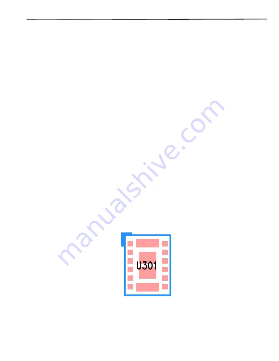
Antenna Swithch Module with SAW Filter : U301
FEM ( Front End Module ) consists of Tx filter, having an antenna port, and dual configuration with the
transmitting path isolated from the receiving path, and Rx saw filter. A signal receives from the antenna
of frequency band which is 881.5±12.5MHz for GSM850 bands, 1842.5±37.5 MHz for DCS bands, and
1960±30 MHz for PCS bands and transmits it to the saw filter for each band. The Tx filter passes
through the output signals of frequency band that is 836.5MHz ±12.5MHz for GSM850 bands,
1747.5±37.5 MHz for DCS bnads, and 1880 ±30 MHz for PCS bands from the power amplifier and
transmits it to the antenna. The maximum insertion loss is about 1.5 dB for the receiving bands at 25
o
C
and about 1.5 dB for the transmitting bands at 25
o
C.
SAW
filter consist of the GSM850 band signals which range 881.5
±
12.5MHz, the DCS band signals
which range 1842.5±37.5, and the PCS bands that cover 1960±30MHz. it degrade other band signals
with high passing loss of 30~60 dB and maximum insertion loss is 2.6 dB
Fig.4-7. Receiver part PCB Layout
Содержание PG-1810
Страница 9: ...PG 1810 Service Manual PANTECH R D CONFIDENTIAL 8 3 4 BLUETOOTH MODULE...
Страница 24: ...PG 1810 Service Manual PANTECH R D CONFIDENTIAL 23 Fig 4 11 Top view of VCTCXO part on the PCB artwork...
Страница 34: ...PG 1810 Service Manual PANTECH R D CONFIDENTIAL 33 CP111 CP115 CP116 CP113 CP112 CP114 CP115 CP115 CP116...
Страница 43: ...PG 1810 Service Manual PANTECH R D CONFIDENTIAL 42 CP137 CP138 CP136...
Страница 45: ...PG 1810 Service Manual PANTECH R D CONFIDENTIAL 44 CP140 CP139 CP141...
Страница 47: ...PG 1810 Service Manual PANTECH R D CONFIDENTIAL 46 CP145...
Страница 50: ...PG 1810 Service Manual PANTECH R D CONFIDENTIAL 49 CP147 CP148 CP149...
Страница 51: ...PG 1810 Service Manual PANTECH R D CONFIDENTIAL 50 CP150...


