32
9.2.2.
RF white balance adjustment
Name of measuring instrument
Connection
Remarks
W/ B pattern
Color analyzer
(Minolta CA-100 or equivalent)
RF input
Panel surface
Steps
Remarks
• Make sure the front panel to be used on the final set is fitted.
• Make sure a color signal is not being shown before adjustment.
• Put the color analyzer where there is little colour variation.
Picture menu : Dynamic
ASPECT : 16:9
Adjustment
Remarks
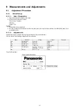
1. Display the white balance pattern.
2. Enter the service adjustment mode.
3. A number key [ 1 ] or [ 2 ] are operated and [ WB-ADJ ] is displayed.
Check that the color balance is [ COOL ].
4. Select [ G-CUTOFF ] item, using the number-key [ 3 ] or [ 4 ], and set to [ 80 ], using the
volume-key [ + ] or [ - ].
Also, [ B-CUTOFF ] and [ R-CUTOFF ] set to [ 80 ]
5. Set [ G-DRIVE ] at [ E0 ](37 inch / 42 inch), [ D0 ](50 inch).
6. Touch the signal receiver of color analyzer to the highlight window's center, and adjust B
drive and R drive so x, y become the [ COLOR TEMP COOL ] in the below table.
7. All RGB drive increase so that the maximum drive value of RGB may become [ FC ].
([ ALL-DRIVE ] set to [ FC ].)
8. Set colorbalance to [ NORMAL ] using [ 7 ] key.
9. Fix G-CUTOFF , B-CUTOFF and R-CUTOFF at [ 80 ].
10. Fix G drive at [ E0 ] (37 inch / 42inch), [ D0 ] (50 inch).
11. Adjust B-DRIVE and R-DRIVE so the highlight window’s x, y become the [COLOR TEMP
NORMAL ] in the below table.
12. All RGB drive increase so that the maximum drive value of RGB may become [ FC ].
([ ALL-DRIVE ] set to [ FC ].)
13. Set colorbalance to [ WARM ] using [ 7 ] key.
14. Fix G-CUTOFF , B-CUTOFF and R-CUTOFF at [ 80 ].
15. Fix G drive at [ E0 ] (37 inch / 42 inch), [ D0 ] (50 inch).
16. Adjust B-DRIVE and R-DRIVE so the highlight window’s x, y become the [ COLOR TEMP
WARM ] in the below table.
17. All RGB drive increase so that the maximum drive value of RGB may become [ FC ].
([ ALL-DRIVE ] set to [ FC ].)
Highlight section Signal amplitude 75% Value is
Hex.
Содержание VIERA TX-P42S10B
Страница 17: ...17 6 4 No Picture ...
Страница 29: ...29 9 1 4 Adjustment Volume Location 9 1 5 Test Point Location ...
Страница 34: ...34 ...
Страница 40: ...40 ...
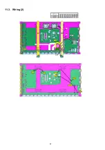
Страница 42: ...42 11 3 Wiring 2 ...
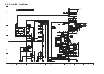
Страница 43: ...43 11 4 Wiring 3 ...
Страница 44: ...44 ...
Страница 45: ...45 12 Schematic Diagram 12 1 Schematic Diagram Note ...
Страница 79: ...79 13 Printed Circuit Board 13 1 P Board A B C D E F G H I 1 2 3 4 5 6 P BOARD FOIL SIDE ETX2MM747MFE ...
Страница 81: ...81 A B C D E F G H I 1 2 3 4 5 6 P BOARD COMPONENT SIDE ETX2MM747MFE ...
Страница 92: ...92 ...
Страница 94: ...94 14 1 2 Packing 1 ...
Страница 95: ...95 14 1 3 Packing 2 ...
Страница 96: ...96 14 1 4 Mechanical Replacement Parts List ...
Страница 100: ...100 14 2 Electrical Replacement Parts List 14 2 1 Replacement Parts List Notes ...


