9
7
6
8
13
12
17
16
19
18
42
44
43
41
36
37
32
30
31
29
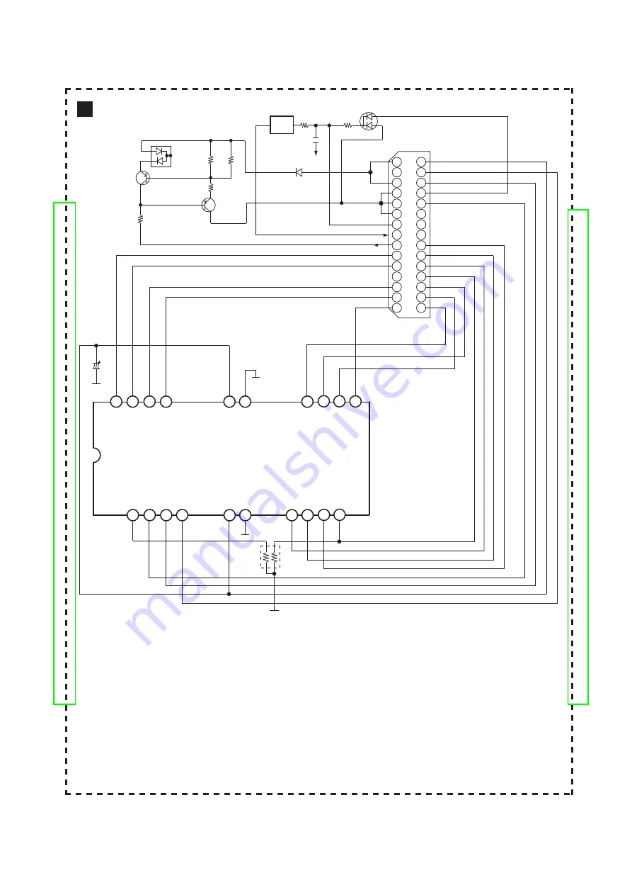
N.C R/B
RE
CE
Vcc Vss
CLE ALE WE WP
I/O
0
I/O
1
I/O
2
I/O
3
Vss
Vcc
I/O
4
I/O
5
I/O
6
I/O
7
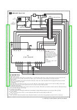
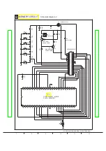
IC2
FLASH MEMORY
15
14
5
7
9
11
13
12
10
8
6
3
4
1
2
17
16
19
18
21
20
23
22
24
CN5
30
28
29
26
27
25
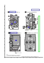
MEMORY BLOCK
B
(TO MAIN CIRCUIT CN1)
D9
KEY
I/O 0 ~ I/O7:
DATA INPUTS/OUTPUTS
The I/O pins are used to input
command,address and data, and
to output data during read operations.
The I/O pins float to high-z when the
chip is deselected or when the
outputs are disabled.
Vcc:
POWER
Vcc is the power supply for device.
Vss: GROUND
CLE: COMMAND LATCH ENABLE
The CLE input controls the activating path for commands sent to the command register. When active high, commands are latched into the command register through
the I/O ports on the rising edge of the WE signal.
ALE: ADDRESS LATCH ENABLE
The ALE input controls the activating path for address to the internal address registers.Addresses are latched on the rising edge of WE with ALE high.
WE: WRITE ENABLE
The WE input controls writes to the I/O port. Commands, address and data are latched on the rising edge of the WE pulse.
WP: WRITE PROTECT
The WP pin provides inadvertent write/erase protection during power transitions. The internal high voltage generator is reset when the WP pin is active low.
PIN DESCRIPTION
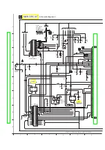
Chargeable Control Pin
5V
Q2
Q3
B1ADMD000012
2SA1774STL
CHARGEABLE
CHARGEABLE
0.68
1.04
0.68
0.69
0.69
1.05
D3
MA3J14700L
Battery
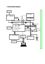
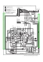
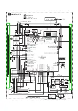
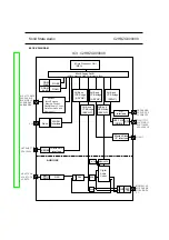
SV-MP720V(GC/GK/GD/GN/GH) BLOCK DIAGRAM
Содержание SV-MP720VGC
Страница 12: ...8 2 Checking Procedures for Font table 12 PDF created with pdfFactory Pro trial version www pdffactory com ...
Страница 14: ...14 PDF created with pdfFactory Pro trial version www pdffactory com ...
Страница 15: ...15 PDF created with pdfFactory Pro trial version www pdffactory com ...
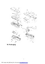
Страница 21: ...18 Packaging 21 PDF created with pdfFactory Pro trial version www pdffactory com ...

