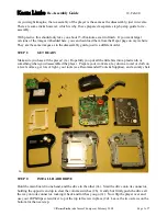
background image

11

7.2.

Replacement for the traverse
motor

• Follow the 

(Step 1)

 - 

(Step 6)

 of item 7.1.1.

NOTE:

Be sure to confirm the item 1.2. “Handling Precautions for
Traverse Deck” before removing the traverse deck ass’y.

7.3.

Replacement for the optical
pick-up

• Follow the 

(Step 1)

 - 

(Step 6)

 of item 7.1.1.

• Follow the 

(Step 1)

 - 

(Step 3)

 of item 7.2.

Содержание SL-SV590EG

Страница 1: ...ectric Industrial Co Ltd All rights reserved Unauthorized copying and distribu tion is a violation of law ORDER NO AD0604011CE Portable CD Player SL SV590EB SL SV590EG SL SV590GC SL SV590GN SL SV590GT Colour S Silver Type ...

Страница 2: ... 2 Location of Controls 7 5 Service Mode 7 5 1 Display of Self Diagnostic Function 7 6 Troubleshooting Guide 8 6 1 Checking the Operation Problems on the Traverse Deck Optical Pick up 8 7 Disassembly and Assembly Instructions 9 7 1 Checking for the PCB 9 7 2 Replacement for the traverse motor 11 7 3 Replacement for the optical pick up 11 7 4 Replacement for the rest switch 13 8 Measurements and Ad...

Страница 3: ...nm Maximum output radiation power from pick up 100 μW VDE Laser radiation from the pick up lens is safety level but be sure the followings 1 Do not disassemble the optical pick up unit since radiation from exposed laser diode is dangerous 2 Do not adjust the variable resistor on the pick up unit It was already adjusted 3 Do not look at the focus lens using optical instruments 4 Recommend not to lo...

Страница 4: ...ustment It has already been adjusted Refer to Fig TR1 Fig TR1 1 2 2 Caution when replacing traverse deck The new traverse deck short circuits by the short pin the foil B and short lands to protect the laser diode against electro static breakdown Be sure to replace to new one following pro cedures 1 Remove the short pin from the FFC and then connect it to the connector 2 Cut the foil B Refer to Fig...

Страница 5: ...ng the equipment for which the lead free solder is used Definition The letter of PbF is printed on the PCB using the lead free solder To put lead free solder it should be well molten and mixed with the original lead free solder Remove the remaining lead free solder on the PCB cleanly for soldering of the new IC Since the melting point of the lead free solder is higher than that of the normal lead ...

Страница 6: ...6 3 Specifications ...

Страница 7: ...isplay below mentioned on the LCD of this unit The substance of self diagnostic display LCD display Press PLAY and STOP button After 15 seconds it is displayed for 2 seconds In case of this display it may be causing for abnormally movements of traverse deck touching failure of REST detect switch and coming off or cutting off the flexible PCB It is necessary for confirmation or repair and replaceme...

Страница 8: ...ry musical program disc 2 Press the skip button to check for normal skip search operation in both the forward and reverse directions 6 1 1 2 Checking manual search 1 Play an ordinary musical program disc 2 Press the manual search button to check for smooth manual search operation at either low or high speed in both the forward and reverse directions 6 1 1 3 Checking playability 1 Play the 0 7 mm b...

Страница 9: ...e major printed circuit boards and replac ing the main components For reassembly after operation checks or replacement reverse the respective procedures Special reassembly procedures are described only when required 7 1 Checking for the PCB 7 1 1 Checking for the PCB A side Check the PCB A side as shown below ...

Страница 10: ...10 7 1 2 Checking for the PCB B side Follow the Step 1 Step 7 of item 7 1 1 Check the PCB B side as shown below ...

Страница 11: ...ep 1 Step 6 of item 7 1 1 NOTE Be sure to confirm the item 1 2 Handling Precautions for Traverse Deck before removing the traverse deck ass y 7 3 Replacement for the optical pick up Follow the Step 1 Step 6 of item 7 1 1 Follow the Step 1 Step 3 of item 7 2 ...

Страница 12: ...12 ...

Страница 13: ...13 7 4 Replacement for the rest switch Follow the Step 1 Step 6 of item 7 1 1 Follow the Step 1 Step 2 of item 7 2 ...

Страница 14: ...s set beyond the limit Check if 1 the waveform or voltage of the focus servo circuit is correct and 2 the optical pick up returns to the normal state by exchanging the traverse deck Follow the below steps when E4 is displayed Cause Focus gain FGC is set beyond the limit Check if 1 the waveform or voltage of the focus servo circuit is correct 2 the focus coil of the optical pick up is correct aroun...

Страница 15: ...ounted on the P C B when it is displayed with mark 2 It is only the Test Round and no terminal Pin is available on the P C B when the TP Test Point indicated as mark 3 The voltage being indicated on the schematic diagram is measured in Standard Playback mode when there is no specify mode is mentioned 4 Although the voltage and waveform available on here is measured with standard frame it may be di...

Страница 16: ...01 55 0 9 1 1 IC501 56 0 9 1 1 IC501 57 0 0 IC501 58 3 3 IC501 59 0 0 IC501 60 0 1 5 IC501 61 3 2 8 IC501 62 0 3 1 IC501 63 2 9 3 IC501 64 0 1 5 IC501 65 0 0 IC501 66 0 0 7 IC501 67 1 5 1 5 IC501 68 0 0 IC501 69 0 2 9 IC501 70 0 0 IC501 71 0 3 1 IC501 72 3 1 3 1 IC501 73 3 1 2 7 IC501 74 3 1 3 1 IC501 75 0 1 6 IC501 76 0 0 IC501 77 1 3 1 3 IC501 78 1 6 1 6 IC501 79 3 1 0 4 IC501 80 0 3 1 IC501 81 ...

Страница 17: ... B2 CHARGE2 B4 B11 30 PDC VC RF OPTICAL PICK UP B2 SL SV590 SV592 BLOCK DIAGRAM VREF RW CD TU 42 1 CRIP MN6627982LC IC501 SERVO PROCESSOR DIGITAL SIGNAL PROCESSOR DIGITAL FILTER D A CONVERTER 52 ARF DSL PLL VCO 72 74 MLD MCLK MCLK MLD 53 IREF 51 DSLF 56 PLLFO 55 PLLF EFM DEMODULATION SYNC INTERPOLATION CIRC ECC CDROM ECC 73 MDATA MDATA 75 STAT STAT MICRO COMPUTER INTERFACE 49 INPUT PORT 47 48 BDO ...

Страница 18: ...K 22 DATA PLL V CC PROGRAM COUNTER PC 18 OUT1 ST PLL GND REFERENCE DIVIDER A FM IN FM GND AM ANT L1102 B5 B5 RF CONT Q1152 1153 B6 C1BB00001070 IC1100 FM AM RF AMP IF DET X1200 B6 X1203 CE MCLK MDATA SWITCH ING QR1202 TREBLE BASS Vol 3 PIN SERIAL CONTROL 26 IN L 27 28 29 30 31 32 NC TREBLEO L BIAS AGC BIAS 1 2 3 4 5 6 7 8 9 10 25 24 23 22 21 11 12 13 14 15 16 TREBLE BASS Vol IN R GND TREBLEO R NC ...

Страница 19: ...S 5 S4 Schematic Diagram S4 1 Interconnection Diagram SIDE A 1 24 OPTICAL PICK UP C 2 R6 LR6 UM 3 BATTERIES 3V CN11 FP101 LCD301 1 15 R1 SL SV590 SV592 WIRING CONNECTION DIAGRAM ...

Страница 20: ...4 34 704 704 34 4 8 8 8 4 8 8 8 5 3 5 8 10 8 10 4 2 4 5 5 5 5 5 5 5 5 5 5 5 6 7 5 5 5 5 2 4 1 1 1 1 1 5 5 5 5 5 5 5 5 5 5 5 0 8 8 857 4 a 0 a4 a176 8 8 a a 37 6a176 2 a 0 2 2 EJ 4EJ 1 176 1 176 56 2 8 4 a8 a4 a 0 a15 a15 6 KP 2 a 0 QWV 0 2 219 4 4 8 10 614 7 4 5 55 5 5 5 5 5 5 5 9 5 5 5 5 5 5 5 855 84 1 8 8 8 1 1 1 5 5 8 10 614 1 614 5 5 5 5 5 5 5 1 a855 5 5 5 5 81 QHH QP 5 2 4 3 5612 81 5 2 a 101...

Страница 21: ... 10 4 6 2 28 648 648 648 648 64 64 5221 52176 0 0 0 0 28 28 59 759 4 2 5 6 4 2 67 1 56 46 4 176 1 8 0 8 8 8 4 857 58 559 28 Q Q Q Q 64 64 10 5246 51 6 52 52 6 855 855 W 8 0 OQWPVa KPa CEM UY 8CTKCVKQP CVGIQT 2 3 3 3 34 34 34 34 34 4 4 4 4 4 4 4 4 4 4 4 4 4 4 4 4 4 4 4 58 2 2 58 0 6 58 4 4 7 4 4 7 4 4 7 4 4 4 704 704 704 704 704 704 704 704 704 704 704 704 0 0 0 4 5 4 7 4 5 4 7 4 5 4 7 2 4 SL SV590...

Страница 22: ...58 58 58 58 58 58 64 52 8 8 8 8 0 0 0 0 0 0 5 1 2 190 5 6 2 6 219 4 4 8 10 614 7 4 51 69 4 a27 a 190 51 69 4 a27 a72 12 0 2 06 2 06 5 5 5 6 2 5 55 5 5 5 5 5 5 5 5 9 5 5 5 5 855 855 855 4 56 4 56 76 219 4 4 5 6 5 5 56 6 4 0 7 5 5 5 5 5 5 5 5 855 855 855 855 84 84 84 1 1 8 8 8 1 1 1 1 1 1 5 5 5 5 8 10 614 1 614 5 5 5 5 5 5 5 5 5 5 1 a855 1 a855 1 a855 5 5 5 5 5 5 5 5 0 4 7 855 855 855 855 7 3 7 3 3 ...

Страница 23: ...04 34 34 704 34 34 704 34 34 704 34 704 34 704 34 704 704 34 34 34 34 4 8 8 8 4 8 8 8 5 3 58 28 28 4 5 6 4 5 6 8 10 8 10 4 2 4 5 219 4 49 6 6 5221 52176 4 5 6 76 76 7 6 56 6 2 2 2 2 2 106 2176 2 0 a2 10 a 28 648 648 5221 52176 0 0 0 28 59 759 4 2 5 6 4 2 67 1 56 46 1 8 0 8 8 8 4 857 857 58 58 559 28 8 0 0 855 855 84 855 855 8 5 6 6 8 8 6 5 66 4 2 0 56 76 W 566 8 0 OQWPVa 20 19 18 17 16 15 14 13 12...

Страница 24: ... 6 6 6 6 6 6 6 6 6 6 6 6 6 6 6 5 5 5 5 5 5 5 5 4 4 4 4 4 4 4 4 4 4 4 4 4 4 4 4 4 4 4 4 4 4 4 4 4 4 4 4 4 4 4 4 4 4 4 4 4 4 4 4 4 4 4 4 4 4 4 4 4 4 4 4 4 3 4 3 4 3 4 3 4 3 3 3 3 3 G 2 G L K J I H M N 1 4 SL SV590EB EG GC GN GT Main P C B Component Side ...

Страница 25: ...S 11 6 6 6 4 4 4 4 4 4 4 4 4 4 4 4 4 4 4 4 4 4 4 4 4 4 4 4 4 4 4 4 4 4 4 4 4 4 4 4 4 4 4 4 4 4 4 4 4 4 4 4 4 4 4 4 4 4 4 4 4 34 34 34 34 34 3 3 3 3 3 3 3 2 4 SL SV590EB EG GC GN GT Main P C B Foil Side ...

Страница 26: ...4 4 4 4 4 4 4 4 4 4 4 4 4 4 4 4 4 4 4 4 4 4 4 4 4 4 4 4 4 4 4 4 4 4 4 4 4 4 4 4 4 4 4 4 4 4 4 4 4 4 4 4 4 4 4 3 4 3 4 3 4 3 4 3 4 3 4 3 3 3 3 G 3 2 2 10 9 8 7 6 5 4 3 2 1 F E D C B A G 11 H 3 4 Component Side Component Side SL SV590EB EG GC GN GT Main P C B ...

Страница 27: ...4 4 4 4 4 4 4 4 4 4 4 4 4 4 4 4 4 4 4 4 4 4 4 4 4 4 4 4 4 4 4 4 4 4 4 4 4 4 4 4 4 4 4 4 4 4 4 4 4 4 4 4 4 4 34 34 34 34 34 3 3 3 3 20 19 18 17 16 15 14 13 12 11 21 4 4 Foil Side SL SV590EB EG GC GN GT Main P C B Foil Side ...

Страница 28: ...S 14 ...

Страница 29: ...TICE Components identified with the mark have the special characteristics for safety When replacing any of these components use only the same type 3 Unless otherwise specified All resistors are in OHMS K 1 000 OHMS All capacitors are in MICRO FARADS uf P uuF 4 The marking RTL indicates the retention time is limited for this item After the discontinuation of this assembly in production it will no l...

Страница 30: ...25V 0 022U 1 C1228 F1H1E183A050 25V 0 018U 1 C112 ECJ1VB1H122K 50V 1200P 1 C1229 F1H1E183A050 25V 0 018U 1 C114 F1H1A105A025 10V 1U 1 C1230 F1H1C104A042 16V 0 1U 1 C116 F1H1E223A029 25V 0 022U 1 C1231 F1H1C104A042 16V 0 1U 1 C117 F1H1E223A029 25V 0 022U 1 C1232 F1H1C104A042 16V 0 1U 1 C120 ECJ1VB1H332K 50V 3300P 1 C1235 F1H1H103A748 50V 0 01U 1 C121 ECJ1VB1H561K 50V 560P 1 C1236 ECJ1VB1H102K 50V 1...

Страница 31: ...0W 0 1 L1301 J0JBC0000019 COIL 1 R532 ERJ3GEYJ100V 1 10W 10 1 R536 ERJ3GEY0R00V 1 10W 0 1 LCD301 L5ACADB00007 LCD 1 R701 ERJ3GEYJ104V 1 10W 100K 1 R703 ERJ3GEYJ100V 1 10W 10 1 PCB1 REP4010B 1M MAIN P C B UNIT 1 RTL R704 ERJ3GEYJ100V 1 10W 10 1 R705 ERJ3GEYJ102V 1 10W 1K 1 Q11 B1BDND000001 TRANSISTOR 1 R706 ERJ3GEYJ102V 1 10W 1K 1 Q12 B1ABMD000004 TRANSISTOR 1 R707 ERJ3GEYJ102V 1 10W 1K 1 Q102 B1DH...

Страница 32: ...ZECH PORTUGUESE S803 EVQ11G05R SW OPERATION 1 A3 RQT8547 K OPERATING INSTRUCTIONS 1 GC CHINESE S804 EVQ11G05R SW OPERATION 1 A3 RQT8548 A OPERATING INSTRUCTIONS 1 GC ARABIC S805 EVQ11G05R SW OPERATION 1 A3 RQT8585 K OPERATING INSTRUCTIONS 1 GT CHINESE S806 EVQ11G05R SW OPERATION 1 A4 K2DA42E00001 POWER PLUG ADAPTOR 1 GC S807 EVQ11G05R SW OPERATION 1 S808 EVQ11G05R SW OPERATION 1 P1 RPFW0013 PROTEC...

Страница 33: ...S7 Exploded View S7 1 Frame and Casing Section S 19 3 17 2 24 25 23 22 21 20 11 8 18 10 14 13 9 7 12 15 6 16 26 5 4 1 19 ...

Страница 34: ...S7 2 Traverse Unit Parts Location S 20 101 5 101 2 101 1 101 7 101 9 101 3 101 8 101 10 101 11 101 4 101 6 101 ...

Страница 35: ...S7 3 Packing Section Except SL SV590GN S 21 P1 P3 A1 A2 A3 P2 Note The configuration of the AC adaptor A1 depend on the area A4 ...

Страница 36: ...S7 4 Packing Section SL SV590GN S 22 P13 P14 A13 P15 P12 A12 P11 A11 ...

Отзывы: