


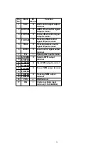


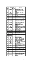


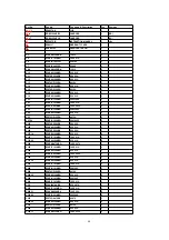
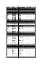


Pin
No.
Mark
I/O
Division
Function
54
SMON3
O
Monitor signal output
terminal (Not used, open)
55
SMON2
O
Monitor signal output
terminal
56
SMON1
O
Monitor signal output
terminal
57
SMON0
O
Monitor signal output
terminal (Not used, open)
58
FSEQ
O
Not used, open
59
VP
O
CLV servo clock judgement
output terminal (Not used,
open)
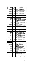
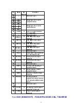
60
FOK
O
Focus OK signal output
terminal
61
DEFECT
O
Defect signal output
teminal (Not used, open)
62
UCLK
O
4.2336MHz/8.4672MHz
output terminal (Not used,
open)
63
VDD1
I
Powe supply terminal
64
VSS
—
GND terminal
65
VDD2
I
Power supply terminal
66
CL
I
CPU interface data clock
input terminal
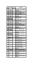
67
CE
I
CPU interface chip enable
signal input terminal
68
DI
I
CPU interface data input
terminal
69
DO
O
CPU interface data output
terminal
70
WRQ
O
CPU interface interrupt
signal output terminal
71
INT
72
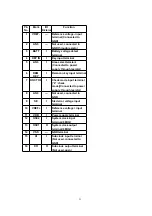
ADIPW0
I
Wobble signal input
terminal
73
RCUT
I
Input terminal for test
(Connected to GND)
74
PCK
O
VCEC clock signal output
terminal
75
VCVDD
I
Power supply terminal for
VCEC
76
FR
I
Bias resistor terminal of
VCEC osillation frequency
(Connected to power
supply through resistor)
28
Содержание SJ-MJ70
Страница 5: ...5 ...
Страница 6: ...6 ...
Страница 7: ...7 ...
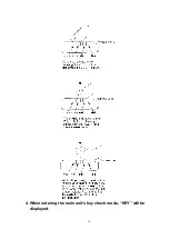
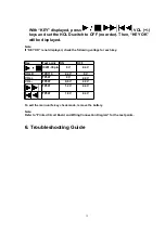
Страница 14: ...4 When entering the main unit s key check mode KEY will be displayed 14 ...
Страница 16: ...16 ...
Страница 17: ...17 ...
Страница 18: ...18 ...
Страница 19: ...19 ...
Страница 20: ...20 ...
Страница 41: ...C309 11 ECUENC333KBQ 16V 0 033U 3 41 ...
Страница 45: ...45 ...
Страница 49: ......
Страница 50: ......
Страница 51: ......
Страница 52: ......
Страница 53: ......
Страница 54: ......
Страница 55: ......
Страница 56: ......
Страница 57: ......
Страница 58: ......
Страница 59: ......
Страница 60: ......
Страница 61: ......
Страница 62: ......
Страница 63: ......
Страница 64: ......
Страница 65: ......
Страница 66: ......


