background image

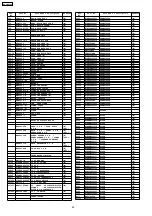
Notes:

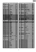
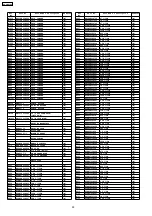
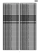
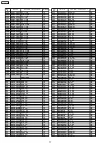
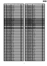
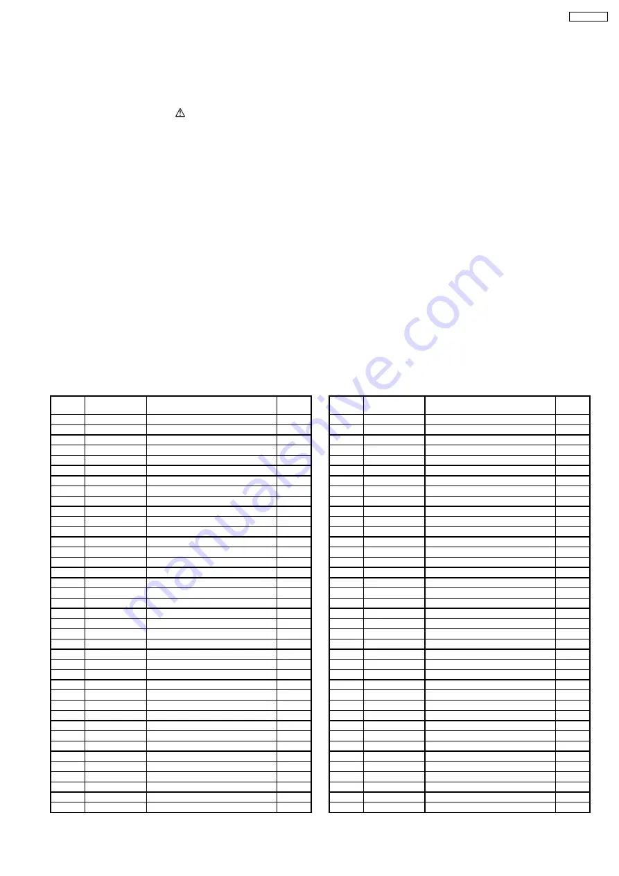
Ref.

No.

Part No.

Part Name & Description

Remarks

CABINET AND CHASSIS

1

REEV0112

19P FFC (DECK-MAIN)

[M]

2

REEV0113

15P FFC

[M]

3

REEV0114

17P FFC (CD-MAIN)

[M]

4

REXV0062

WIRE 8P (PWR-TRAN)

[M]

5

RFKGAPM33EBS

FRONT PANEL ASS’Y

[M]

6

RGKV0149-S

VOLUME ORNAMENT

[M]

7

RGLV0061-Q

LIGHTING TIP

[M]

8

RKSV0035-H

REAR CABINET

[M]

9

RGU2280-S

CASS EJECT BUTTON

[M]

10

RGUV0134C-S

FUNCTION BUTTON

[M]

11

RGUV0156-S

POWER BUTTON

[M]

12

RGUV0157-S

STOP BUTTON

[M]

13

RGUV0158-S

CD EJECT BUTTON

[M]

14

RGUV0159-S

CONTROL BUTTON

[M]

15

RGWV0039-S

VOLUME KNOB

[M]

16

RHD26046-L

SCREW

[M]

17

RMNV0062

FL HOLDER

[M]

18

RHDV30005

SCREW

[M]

19

RHDV30007

SCREW

[M]

20

RHGV0008

LEG CUSHION

[M]

21

RKF0688-S

CASS HOLDER/LID

[M]

22

RKFV0059-S

CD LID

[M]

23

RKMV0064-H

SIDE PANEL (L)

[M]

24

RKMV0065-H

SIDE PANEL (R)

[M]

25

RKMV0066-S

TOP CABINET

[M]

26

RMAV0001

MAIN PCB SUPPORT

[M]

27

RMB0448-J

LOCK ROD SPRING

[M]

28

RMBV0046

CASS LID OPEN SPRING

[M]

29

RMKV0051

BOTTOM CHASSIS

[M]

30

RMM0163-1

CASSETTE LOCK ROD

[M]

31

RSCV0073

REAR SHIELD

[M]

32

RUS757ZAA

CASS HALF SPRING

[M]

33

RXGX0002

DAMPER GEAR

[M]

34

RXXV0040

HEAT SINK UNIT

[M]

35

SHE187-4J

POWER PCB SUPPORT

[M]

36

RWJ1104150QX

4P WIRE

[M]

37

XTB3+10JFJ

SCREW

[M]

Ref.

No.

Part No.

Part Name & Description

Remarks

38

XTB3+20JFJK

SCREW

[M]

39

XTB3+8FFJ

SCREW

[M]

40

XTV3+10GFJ-M

SCREW

[M]

41

XTV3+8FFJ

SCREW

[M]

42

RWJ1105205QX

5P WIRE (PANEL-TRAN)

[M]

CASSETTE DECK

101

RED0067-2

R/P HEAD BLOCK UNIT

[M]

103

RDG0300

REEL BASE GEAR

[M]

104

RDG0301

WINDING RELAY GEAR

[M]

105

RDK0026-4

MAIN GEAR

[M]

107

RDV0033-4

WINDING BELT

[M]

108

RDV0064-1

CAPSTAN BELT

[M]

110

RMB0312

TRIGGER LEVER SPRING

[M]

111

RMB0400

REEL SPRING

[M]

112

RMB0403

HEAB PANEL SPRING

[M]

113

RMB0404

BRAKE ROD SPRING

[M]

114

RMB0406-5

FR LEVER SPRING

[M]

115

RMB0408

THRUST SPRING

[M]

116

RML0370-4

TRIGGER LEVER

[M]

117

RML0371

FR LEVER

[M]

118

RML0372-2

WINDING LEVER

[M]

119

RML0374-2

EJECT LEVER

[M]

120

RMM0131-1

BRAKE ROD

[M]

121

RMM0133-1

EJECT ROD

[M]

122

RMQ0519

REEL HUB

[M]

123

RMS0398-1

MOVING CORE

[M]

124

RXQ0470-2

PLUNGER

[M]

125

RMC0061

PACK SPRING

[M]

126

RXF0061-1

FLYWHEEL F ASS’Y

[M]

128

RXG0040

FF RELAY GEAR ASS’Y

[M]

129

RMK0283A-2

SUB-CHASSIS

[M]

130

RXL0124

PINCH ROLLER F ASS’Y

[M]

130-1

RMB0401

PINCH ARM SPRING F

[M]

132

RXL0126

WINDING ARM ASS’Y

[M]

133

RXQ0412-3

HEAD PANEL ASS’Y

[M]

133-1

RMB0405-1

FR ROD SPRING

[M]

133-2

RMM0132-1

FR ROD

[M]

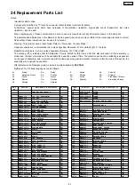
24 Replacement Parts List


·


Important safety notice:

Components identified by

mark have special characteristics important for safety.

Furthermore, special parts which have purposes of fire-retardent (resistors), high-quality sound (capacitors), low noise
(resistors), etc are used.
When replacing any of these components, be sure to use only manufacturer’s specified parts shown in the parts list.


·


The parenthesized indications in the Remarks columns specify the areas or colour. (Refer to the cover page for area or colour)

Parts without these indications can be used for all areas.


·


Warning: This product uses a laser diode. Refer to “Precaution of Laser Diode”.


·


Capacitor values are in microfarads (µF) unless specified otherwise, P= Pico-farads (pF), F= Farads.


·


Resistance values are in ohms, unless specified otherwise, 1K=1,000 (OHM).


·


The marking (RTL) indicates that the Retention Time is limited for this items. After the discontinuation of this assembly in
production, the item will continue to be available for a specific period of time. The retention period of a availability is dependent
on the type of assembly, and in accordance with the laws governing part and product retention. After the end of this period, the
assembly will no longer be available.


·


[M] Indicates in the Remarks columns indicates parts supplied by

PAVCSG.


·


Reference for O/I book languages are as follows:

Ar:

Arabic

Du:

Dutch

It:

Italian

Sp:

Spanish

Cf:

Canadian French

En:

English

Ko:

Korean

Sw:

Swedish

Cz:

Czech

Fr:

French

Po:

Polish

Co:

Traditional Chinese

Da:

Danish

Ge:

German

Ru:

Russian

Cn:

Simplified Chinese

Pe:

Persian

Ur:

Ukraine

87

SA-PM33EE

Содержание SA-PM33EE

Страница 1: ...Co Ltd All rights reserved Unauthorized copying and distribution is a violation of law SA PM33EE Colour S Silver Type S N 20 dB at 999 kHz 1122 µV m n Cassette Deck Section Track system 4 track 2 channel Heads Record playback Solid permalloy head Erasure Double gap ferrite head Motor DC servo motor Recording system AC bias 100 kHz Erase system AC erase 100 kHz Tape speed 4 8 cm s Overall frequency...

Страница 2: ...Mass 3 5 kg Operating temperature range 5 to 35 C Operation humidity range 5 to 90 RH no condensation Power consumption in standby mode 0 8 W Notes 1 Specifications are subject to change without notices Mass and dimensions are approximate 2 Total harmonic distortion is measured by the digital spectrum analyzer n System SC PM33EE S Music center SA PM33EE S Speaker SB PM33EG M 9 12 Disassembly of Ma...

Страница 3: ... Transformer Circuit Headphone Circuit and Speaker Terminal Circuit 69 19 Printed Circuit Board 71 19 1 CD Servo P C B 71 19 2 Main P C B and Tuner Extent P C B 72 19 3 Panel P C B 73 19 4 Deck P C B Deck Mechanism P C B and Tape Eject P C B 74 19 5 Power P C B and Speaker Terminal P C B 75 19 6 Transformer P C B and Headphone P C B 76 20 Illustration of IC s Transistors and Diodes 77 21 Terminal ...

Страница 4: ...s not have a return path to the chassis the reading must be Figure 1 1 1 2 Leakage Current Hot Check See Figure 1 1 Plug the AC cord directly into the AC outlet Do not use an isolation transformer for this check 2 Connect a 1 5kΩ 10 watts resistor in parallel with a 0 15µF capacitors between each exposed metallic part on the set and a good earth ground such as a water pipe as shown in Figure 1 3 U...

Страница 5: ...y have operated if either of the following conditions are noticed No sound is heard when the power is turned on Sound stops during a performance The function of this circuitry is to prevent circuitry damage if for example the positive and negative speaker connection wires are shorted or if speaker systems with an impedance less than the indicated rated impedance of the amplifier are used If this o...

Страница 6: ...ssembly 3 Use only a grounded tip soldering iron to solder or unsolder ES devices 4 Use only an anti static solder remover device Some solder removal devices not classified as anti static ESD protected can generate electrical charge to damage ES devices 5 Do not use freon propelled chemicals These can generate electrical charges sufficient to damage ES devices 6 Do not remove a replacement ES devi...

Страница 7: ...riable resistor on the pickup lens 4 Do not disassemble the optical pick up unit 5 If the optical pick up is replaced use the manufacturer s specified replacement pick up only 6 Use of control or adjustments or performance of procedures other than those specified herein may result in hazardous radiation exposure CAUTION THIS PRODUCT UTILIZES A LASER USE OF CONTROLS OR ADJUSTMENTS OR PERFORMANCE OF...

Страница 8: ...variable resistor laser power adjustment It has already been adjusted Fig 4 1 l Grounding for electrostatic breakdown prevention 1 Human body grounding Fig 4 2 Use the anti static wrist strap to discharge the static electricity from your body 2 Work table grounding Fig 4 2 Put a conductive material sheet or steel sheet on the area where the traverse deck optical pickup is placed and ground the she...

Страница 9: ... the melting point is 50 70 F 30 40 C higher Please use a high temperature soldering iron In case of soldering iron with temperature control please set it to 700 20 F 370 10 C Pb free solder will tend to splash when heated too high about 1100 F 600 C When soldering or unsoldering please completely remove all of the solder on the pins or solder area and be sure to heat the soldering points with the...

Страница 10: ...Remote control AC cord FM indoor antenna AM loop antenna 6 Accessories Note Refer to Packing Materials Accessories Section 24 for part number 10 SA PM33EE ...

Страница 11: ...7 Operating Instructions Procedures 7 1 Main Unit Remote Control Operation 11 SA PM33EE ...

Страница 12: ...7 2 Disc Information 12 SA PM33EE ...

Страница 13: ...ow by 4 and 7 on remote control To exit press button on main unit or remote control FL Display Test To check the FL segments display All segments will light up In doctor mode 1 Press DIMMER button on remote control To exit press button on main unit or remote control CD to Tape Recording Test Mode To Inspect the recording process from CD to TAPE for the unit For more information refer to section 8 ...

Страница 14: ...following F REC INH SW is ON HALF SW is ON TPS signal changes After checking TPS it shall STOP If TPS checking is completed at TAPE END it is considered as TPS abnormal 5 REC key is pressed after loading in a NORMAL type cassette with both recording tabs intact REC operation shall not be executed Check the following F REC INH SW is ON HALF SW is ON 6 Self diagnostic mode is stopped by pressing the...

Страница 15: ...s at constant analogue recording speed for 3 seconds Stop However Error would be display if there is no tracks to access to no tape inserted no test CD inserted or when the tape erasure prevention tab for FWD side is not suitable for recording When in this mode if button is pressed the process will stops automatically 8 1 4 Tape Recording and Playing Purpose To check the Tape function Assuming the...

Страница 16: ... button on remote control Enter into TPS Test mode During this mode Software will start checking for existence of cassette in Deck If the Deck does not contain any cassette it shall end the test and displays the result of the test The test will start by playing the Deck in forward direction for 1 sec and then FF TPS If TPS signal is OK the Deck shall be ejected Below is information on the TPS unde...

Страница 17: ...y Remarks H01 MODE SW abnormal For deck mechanism unit Press on main unit for next error H02 REC INH SW abnormal For deck mechanism unit Press on main unit for next error H03 HALF SW abnormal For deck mechanism unit Press on main unit for next error F01 F02 Reel pulse abnormal TPS abnormal For deck mechanism unit Press on main unit for next error F15 CD REST SW Abnormal CD traverse position intial...

Страница 18: ...erse Press on main unit for next error POWER AMP output abnormal During normal operation if DCDET becomes L normal POWER OFF process shall not be executed PCONT shall be switched to L immediately GOODBYE shall not be display but the error display F61 is displayed instead 2 seconds after the F61 displayed ECONO shall be set to L and FL display shall be turned off The error content shall be memorize...

Страница 19: ...embly of Side Panel L R Disassembly of Top Cabinet Unit Disassembly of Deck Mechanism and Tape Eject P C B Disassembly of Headphone P C B Disassembly of Front Panel Disassembly of Panel P C B Disassembly of Rear Panel Disassembly of Tuner Pack Disassembly of Main P C B Disassembly of Power P C B Disassembly of Speaker Terminal P C B Disassembly of Transformer P C B Disassembly of CD Mechanism Disa...

Страница 20: ... chart The following chart is the procedure for disassembling the casing and inside parts for internal inspection when carrying out the servicing To assemble the unit reverse the steps shown in the chart below 20 SA PM33EE ...

Страница 21: ...9 3 Main Parts Location Diagram 21 SA PM33EE ...

Страница 22: ...ow shown Disassembly of Side Panel L Step 3 Remove 5 screws Step 4 Remove the side panel L as arrow shown 9 5 Disassembly of Top Cabinet Unit Step 1 Remove 3 screws Step 2 Remove 3 screws Step 3 Lift up the top cabinet unit push backward as arrow shown and flip top cabinet unit sideway Be careful of the catch 22 SA PM33EE ...

Страница 23: ... clutch Step 3 Remove the Tape Eject P C B Disassembly of Deck Mechanism Step 4 Remove 4 screws Step 5 Push the lever as arrow shown to open the cassette lid Step 6 Remove the Deck Mechanism 9 7 Disassembly of Headphone P C B Follow the Step 1 Step 6 of Item 9 5 Step 1 Remove 1 screw Step 2 Release the clutch Step 3 Remove the Headphone P C B 9 8 Disassembly of Front Panel Follow the Step 1 Step 4...

Страница 24: ...nnect FFC cable CN901B Step 3 Release 3 claws Step 4 Remove the Front Panel as arrow shown 9 9 Disassembly of Panel P C B Follow the Step 1 Step 4 of Item 9 4 Follow the Step 3 Step 6 of Item 9 5 Follow the Step 1 Step 4 of Item 9 8 24 SA PM33EE ...

Страница 25: ... Panel as arrow shown 9 11 Disassembly of Tuner Pack Follow the Step 1 Step 4 of Item 9 4 Follow the Step 3 Step 6 of Item 9 5 Follow the Step 1 Step 2 of Item 9 10 Step 1 Detach the connector CN401A and remove the tuner pack as arrow shown 9 12 Disassembly of Main P C B Follow the Step 1 Step 4 of Item 9 4 Follow the Step 1 Step 6 of Item 9 5 Follow the Step 1 step 4 of Item 9 8 Follow the Step 1...

Страница 26: ... P C B Follow the Step 1 Step 4 of Item 9 4 Follow the Step 4 Step 6 of Item 9 5 Follow the Step 1 Step 2 of Item 9 10 Step 1 Detach the connector CN505B Step 2 Remove 1 screw Step 3 Detach the connector CN501A CN508A and CN503A Step 4 Remove the Power P C B as arrow shown Replacement of Power Amplifier IC Step 5 Remove 3 screws 26 SA PM33EE ...

Страница 27: ... Release the clutch Step 3 Remove the Speaker Terminal P C B as arrow shown 9 15 Disassembly of Transformer P C B Follow the Step 1 Step 4 of Item 9 4 Follow the Step 4 Step 6 of Item 9 5 Follow the Step 1 Step 2 of Item 9 10 Follow the Step 1 Step 4 of Item 9 13 Step 1 Detach the connector CN900B Step 2 Remove 4 screws Step 3 Remove the Transformer P C B as arrow shown 9 16 Disassembly of CD Mech...

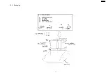
Страница 28: ...e Lid Follow the Step 1 Step 2 of Item 9 4 Follow the Step 3 Step 6 of Item 9 5 Follow the Step 1 step 4 of Item 9 6 Step 1 Using screwdriver to remove Damper gear as arrow shown Step 2 Remove the Cassette Open Spring as arrow shown in order Step 3 Pull the sides Cassette holders to the direction of the arrows shown 28 SA PM33EE ...

Страница 29: ...anism Unit 9 18 1 Disassembly of the Traverse Unit Follow the Step 1 Step 4 of Item 9 4 Follow the Step 4 Step 6 of Item 9 5 Follow the Step 1 Step 4 of Item 9 8 Follow the Step 1 Step 2 of Item 9 10 Follow the Step 1 Step 4 of Item 9 12 Follow the Step 1 Step 3 of Item 9 16 Disassembly of gears drive 29 SA PM33EE ...

Страница 30: ...30 SA PM33EE ...

Страница 31: ...31 SA PM33EE ...

Страница 32: ...Step 1 Step 4 of Item 9 4 Follow the Step 4 Step 6 of Item 9 5 Follow the Step 1 Step 4 of Item 9 8 Follow the Step 1 Step 2 of Item 9 10 Follow the Step 1 Step 4 of Item 9 12 Follow the Step 1 Step 3 of Item 9 16 Follow the Step 1 Step 4 of Item 9 18 1 32 SA PM33EE ...

Страница 33: ...Follow the Step 1 Step4 of Item 9 4 Follow the Step 4 Step 6 of Item 9 5 Follow the Step 1 Step 4 of Item 9 8 Follow the Step 1 Step 2 of Item 9 10 Follow the Step 1 Step 4 of Item 9 12 Follow the Step 1 Step 3 of Item 9 16 Follow the Step 1 Step 2 of Item 9 18 1 33 SA PM33EE ...

Страница 34: ...Step 1 Step 6 of Item 9 5 Follow the Step 1 Step 6 of Item 9 6 9 22 Disassembly of Motor Capstan Belt A Capstan Belt B and Winding Belt Deck Mechanism Unit Follow the Step 1 Step 6 of Item 9 5 Follow the Step 1 Step 6 of Item 9 6 Follow the Step 1 Step 4 of Item 9 21 34 SA PM33EE ...

Страница 35: ...35 SA PM33EE ...

Страница 36: ...f Deck Mechanism P C B Follow the Step 1 Step 6 of Item 9 5 Follow the Step 1 Step 6 of Item 9 6 Follow the Step 1 Step 4 of Item 9 21 9 24 Handling of cassette tape jam Follow the Step 1 Step 4 of Item 9 4 36 SA PM33EE ...

Страница 37: ...nsion P C B A Main P C B Speaker Terminal P C B RFKZPM33E 11 Service Positions Note For description of the disassembly procedures see the Section 9 11 1 Checking and Repairing of Deck Deck Mechanism Headphone P C B and Tape Eject P C B 37 SA PM33EE ...

Страница 38: ...11 2 Checking and Repairing of Panel P C B 38 SA PM33EE ...

Страница 39: ...11 3 Checking and Repairing of Tuner Pack P C B 39 SA PM33EE ...

Страница 40: ...11 4 Checking and Repairing of Transformer P C B 40 SA PM33EE ...

Страница 41: ...11 5 Checking and Repairing of Main P C B 41 SA PM33EE ...

Страница 42: ...11 6 Checking and Repairing of CD Mechanism P C B 42 SA PM33EE ...

Страница 43: ...11 7 Checking and Repairing of Speaker Terminal P C B 43 SA PM33EE ...

Страница 44: ...11 8 Checking and Repairing of Power P C B 44 SA PM33EE ...

Страница 45: ...al timing at STOP mode ON approx 200msec e REV REW Supply the plunger power in a flash at REV PLAY mode ON approx 50msec f STOP Supply the plunger power in a flash at FF mode ON approx 50msec Repeat the operation FWD PLAY Note Other operation may start if a timing of supplying the plunger power is missed 12 1 1 Connection Status between Mechanism and Power Supply Motor Plunger 12 1 2 Operative Par...

Страница 46: ...Fig 7 46 SA PM33EE ...

Страница 47: ...bling 2 Remove 4 screws from the mechanism unit to disassemble under 9 Assembling and Disassembling 3 Connect the headphone jack output jig Fig 8 to headphone jack Fig 8 Fig 9 13 1 4 Tape Speed Adjustment Normal speed adjustment only during forward playback Product reference value 3 000 90Hz 1 Connect a frequency indicator Fig 10 2 Playback the middle portion of the test tape QZZCWAT 3 Adjust the ...

Страница 48: ...use the recording mode Repeat pressing the buttons till the recording pause mode is activated 5 Check that the output level is within the standard range Standard Range 16 3mV Fig 12 13 1 6 Bias Frequency Check 1 Connect a digital frequency counter Fig 13 2 Set the function to TAPE position 3 Insert a normal blank cassette tape QZZCRA and press REC mode on main unit 4 Check that the output frequenc...

Страница 49: ...1 6 1 6 1 6 2 2 1 4 1 8 1 8 STANDBY 0 0 0 0 0 0 0 4 0 0 2 0 2 0 0 0 2 0 0 0 0 2 0 2 0 2 0 2 Ref No MODE 41 42 43 44 45 46 47 48 49 50 51 52 53 54 55 56 57 58 59 60 CD PLAY 0 2 2 4 0 1 8 1 2 1 8 3 3 1 2 1 2 1 2 1 7 1 9 0 8 1 5 1 4 0 0 3 1 5 0 STANDBY 0 0 3 0 0 0 2 0 1 0 3 0 4 0 2 0 2 0 1 0 1 0 3 0 0 0 0 0 4 0 0 Ref No MODE 61 62 63 64 65 66 67 68 69 70 71 72 73 74 75 76 77 78 79 80 CD PLAY 3 3 0 0 ...

Страница 50: ...8 4 8 4 8 1 1 4 8 0 4 6 4 6 0 0 0 2 STANDBY 0 0 0 0 0 4 8 2 8 0 0 0 0 0 4 8 0 0 0 0 0 0 0 Ref No MODE 41 42 43 44 45 46 47 48 49 50 51 52 53 54 55 56 57 58 59 60 CD PLAY 1 1 0 1 0 0 3 0 1 0 0 1 0 4 7 2 4 0 1 3 4 4 0 0 0 0 0 0 0 STANDBY 0 0 0 0 0 1 0 0 1 0 0 2 4 0 2 1 0 0 0 0 0 0 0 0 Ref No MODE 61 62 63 64 65 66 67 68 69 70 71 72 73 74 75 76 77 78 79 80 CD PLAY 0 0 0 0 0 0 0 0 0 0 0 0 0 4 7 4 1 6 ...

Страница 51: ...CD PLAY 20 9 20 9 4 9 0 STANDBY 21 2 21 2 0 0 PANEL P C B IC900 IC900 IC900 14 1 4 Power P C B Ref No MODE 1 2 3 4 5 6 7 8 9 10 11 12 CD PLAY 23 4 11 4 0 11 4 4 6 0 0 0 4 2 11 4 0 11 4 STANDBY 2 9 0 3 0 0 3 0 0 0 0 0 0 3 0 0 3 Ref No MODE E C B E C B E C B E C B E C B CD PLAY 23 3 20 23 3 5 20 5 6 20 8 9 7 20 3 5 9 6 5 6 4 8 7 5 5 5 STANDBY 4 3 2 4 4 3 2 4 2 5 3 2 2 9 0 2 2 5 2 4 0 2 0 1 0 0 0 Ref...

Страница 52: ...C B E C B CD PLAY 0 0 0 7 0 0 0 7 1 9 1 8 0 0 6 8 0 6 8 0 6 8 STANDBY 0 0 0 7 0 0 0 7 19 8 1 8 0 0 0 1 0 0 1 0 0 1 Ref No MODE E C B E C B E C B E C B E C B CD PLAY 0 9 7 0 1 0 9 7 0 0 0 0 9 7 1 1 9 7 9 6 0 9 7 STANDBY 0 0 1 0 0 0 1 0 0 0 0 0 0 0 1 0 1 0 0 1 Ref No MODE E C B E C B CD PLAY 0 9 1 1 0 0 0 STANDBY 0 0 0 0 0 0 Q1316 Q1317 Q1304 Q1309 Q1310 Q1312 Q1314 Q1315 Q1101 Q1201 Q1302 Q1303 DEC...

Страница 53: ...Vp p 100nsec div IC803 PIN 13 CD PLAY 2 8Vp p 100nsec div IC803 PIN 15 CD PLAY 2 24Vp p 25usec div IC803 PIN 16 CD PLAY 4 96Vp p 10usec div IC803 PIN 22 CD PLAY 1 07Vp p 10msec div IC803 PIN 23 CD PLAY 4 6Vp p 10msec div IC803 PIN 27 CD PLAY 4 72Vp p 10msec div CN801 PIN 6 CD PLAY 3 12Vp p 10msec div IC803 PIN 30 CD PLAY 5 04Vp p 10msec div IC803 PIN 36 CD PLAY 4 88Vp p 10msec div IC803 PIN 40 CD ...

Страница 54: ...N 56 CD PLAY 528mVp p 2 5msec div CN7001 PIN 59 CD PLAY 512mVp p 1msec div CN7001 PIN 68 CD PLAY 3 8Vp p 10msec div CN7001 PIN 69 CD PLAY 1 96Vp p 10msec div CN7001 PIN 70 CD PLAY 3 52Vp p 10msec div CN7001 PIN 71 CD PLAY 3 28Vp p 10msec div CN7001 PIN 74 CD PLAY 4Vp p 250nsec div CN7001 PIN 24 CD PLAY 3 08Vp p 25usec div CN7001 PIN 80 CD PLAY 4 48Vp p 50nsec div CN7001 PIN 81 CD PLAY 2 64Vp p 50n...

Страница 55: ... PbF SOLDER SIDE PbF SOLDER SIDE PbF PbF SOLDER SIDE 1 8 1 5 1 10 1 4 19 1 18 2 13 1 9 1 1 17 2 16 4 1 1 10 1 10 15 1 14 2 1 8 1 5 1 17 2 16 2 1 1615 9 1 4 1 13 1 14 2 15 1 Tuner Pack CD OPEN SW CP1902 JW1903 CP1301 CN1303 JW308B 1 2 E DECK P C B PbF SOLDER SIDE 1 2 3 4 5 1 9 19 1 18 2 MOTOR 1 2 JW308A 1 2 CN10 CN11 FL900 VR900 CN901A Z901 WH900 JK303 WH505A CN508B CN503B CN501B SPEAKERS I SPEAKER...

Страница 56: ...SA PM33EE 56 ...

Страница 57: ...D1 12 D1 11 M7302 SPINDLE MOTOR B FOCUS COIL TRACKING COIL T OPTICAL PICKUP PHOTO DETECTOR SEMICONDUCTOR LASER F F T Q7601 SWITCH PC1 4 PC B M M X7201 IC7001 MN6627954MA LSI IC TO MAIN BLOCK A LD_SW 81 80 25 24 23 22 21 SPOUT PC TRVP TRP FOP BLKCK TX NRST MLD MCLK MDATA STAT 69 67 68 70 SPOUT PC TRVP TRP FOP X1 X2 BLKCK TX NRST MLD MCLK MDATA STAT LOADING 71 40 C E E E E E F E F D C A B D C 38 B 3...

Страница 58: ...REJECTION MUTE Q1309 Q1310 Q1312 L1301 D1301 Q1317 BEAT PROOF LEVEL SWITCH DECK 2 ERASE HEAD DECK 2 R P HEAD LCH S971 MODE S972 HALF S975 RECIN_H Q1304 Q1101 Q1201 MUTING SWITCH SWITCH DECK MUTING CONT BIAS SWITCH 78 DMT M Q1315 SWITCH D951 70 MOTOR_H MOTOR SWITCH SWITCH MOTOR SUPPLY 71 PL_H PLUNGER SWITCH Q808 Q807 96 VOL_JOG1 97 VOL_JOG2 61 E_DATA E_CLK E_CS 5 D1 62 4 E_CLK 63 3 E_CS 66 STEREO 6...

Страница 59: ...TCH D609 Q503 STABALIZER Q501 SWITCH Q504 SWITCH Q530 Q507 REGULATOR Q505 21 CD_MDATA 22 CD_STAT 23 CD_MCLK 28 CD_OPEN_SW 30 BLKCK 35 CD RST 36 CD_MLD Q801 SWITCH Q802 SWITCH 25 PCONT_1 Z600 MDATA STAT MCLK BLKCK NRST MLD 42 Q500 CURRENT LIMITTING GRID1 GRID11 14 29 21 9 MUTE 12 2 OUT_L OUT_R 5 STBY 8 6 IN_L IN_R 49 10 4 OUT_L OUT_R PCONT_2 D751 REGULATOR REGULATOR 1 VCC FP352 D382 D383 8 9 VOL_DE...

Страница 60: ...SA PM33EE 60 ...

Страница 61: ...Accordingly there may arise some error in voltage values and waveforms depending upon the internal impedance of the tester or the measuring unit Importance safety notice Components identified by mark have special characteristics important for safety Furthermore special parts which have purposes of fire retardant resistors high quality sound capacitors low noise resistors etc are used When replacin...

Страница 62: ...62 SA PM33EE ...

Страница 63: ...0 0 1 C7626 0 1 R7315 3 3K R7325 330 IC7002 BA5948FPE2 4 CH DRIVE VCC NC NC NC IN3 IN4 VREF NC GND GND PVCC2 PGND2 D4 D4 D3 D3 PGND1 PVCC1 NC D2 D2 D1 D1 IN1 NC NC PC2 PC1 IN2 NC 3 4 5 6 24 25 26 27 28 8 1 2 23 21 9 20 10 19 1 11 18 2 13 17 16 15 22 7 14 R7339 1K A 12 11 10 2 4 6 8 9 7 5 3 1 13 14 15 16 CN7001 CP701 1 2 3 4 5 6 7 8 9 26 27 28 29 30 31 32 33 34 67 68 69 70 71 72 73 74 75 92 93 94 9...

Страница 64: ... 3V1000 C837 6 3V100 C838 6 3V100 R857 4 7K X802 X801 R821 470K C816 16V10 D802 B0ACCK000005 R892 100K R896 1K Q808 Q807 B1GBCFGJ0016 MOTOR SWITCH DEMO L ON H OFF PCONT_2 NC CL NC SDA FL_CLK NC FL_DATA NC FL_CS NC NC NC CD_MLD CD_RST NC NRST NC NC BLKCK REST_SW CD_OPEN_SW HALT RMT REC_H NC DMT TYPE_SELECT NC NC NC NC NC NC NC NC NC NC MP1 MP2 CRTIMER NC S W RST VREF VOL_JOG1 VOL_JOG2 CLOSE_L OPEN_...

Страница 65: ...YS6V CD_7 5V PGND REC1 REC2 MNF1 MOUT1 MNF2 MOUT2 BNF1 BOUT1 BNF2 BOUT2 LEFT RIGHT CAP VCC S1 SC VIN1 SEL1OUT VIN2 SEL2OUT A1 A2 B1 B2 C1 C2 D1 D2 E1 E2 FILTER GND IC800 C1BB00000732 ASP IC R410 1K IC800 CN901B Q803 Q751 C369 100 C361 100 AGND AGND RDS_CLK RDS_DATA DET MUTEB D5V R885 100K R886 1K R888 1K R887 1K C861 330P C860 16V10 C868 6 3V47 C862 16V10 X803 H0H433400002 C866 1000P C863 560P C86...

Страница 66: ...ORT C211 1000P C411 1000P R412 1 8K D906 B3AAA0000489 STANDBY LED Z901 B3RAD0000125 REMOTE SENSOR VR900 EVEJ1CF3024B VOLUME JOG R925 100K C921 100P C920 100P R924 100K C922 6 3V47 R911 1 5K R912 2 2K R913 3 3K R914 4 7K R901 1 2K R902 1 5K R903 2 2K R904 3 3K R905 4 7K C910 50V22 C909 50V22 R922 68 R923 68 D900 B0BC5R600003 KEY1 KEY2 RMT VOL_JOG1 VOL_JOG2 SYS6V VREF WH900 CN901A SCHEMATIC DIAGRAM ...

Страница 67: ...0V1 R1202 1 5K C1204 0 027 C1207 1500P C1206 50V2 2 R1204 10K C1222 0 01 C1208 16V10 R1305 10K C1305 16V33 C1308 16V22 R1307 22 R1308 22 C1109 50V3 3 C1210 6800P R1206 100K R1207 1K R1209 1K R1313 10K C1310 50V0 1 R1309 470 R1110 33K R1210 33K R1107 1K R1109 1K R1205 2 2K C1110 6800P R1106 100K R1105 2 2K C1209 50V3 3 R1371 22K AN6 AN7 VREF VREF PLVCC GND2 PHOTO VREF VREF MODE HALF PL PL_GND PHOTO...

Страница 68: ...C521 0 01 R504 220 D502 C522 0 01 C512 0 1 D501 D501 D502 D504 D505 D0EAMM000038 C523 0 01 D504 C524 0 01 D505 C510 25V10 C507 0 01 VCC SYS6V R505 100K C501 35V6800 D527 D525 D526 D527 B0EAKM000117 D526 D525 R501 1 2 R502 1 2 R503 1 2 Q501 Q504 B1AACF000063 SWITCH Q503 B1BCCG000002 STABILIZER Q500 B1GCCFGA0006 CURRENT LIMITING Q503 Q501 Q504 Q500 AMP_VCC1 AMP_VCC2 AMP_VCC2 AMP_VCC1 MOTOR_9V PCONT_...

Страница 69: ...PM33EE SPEAKER TERMINAL TRANSFORMER HEADPHONE CIRCUIT TRANSFORMER CIRCUIT TO POWER CIRCUIT WH505A ON SCHEMATIC DIAGRAM 6 TO PANEL CIRCUIT WH900 ON SCHEMATIC DIAGRAM 4 C371 0 1 ZJ01 L300 L301 L303 L302 L300 303 G0AR76Y00002 C362 100P C363 100P CN501A CN508A CN803A CN808A JK501 3 1 2 4 R230 100K C230 0 01 HP_SW HP_L HP_GND HP_R WH504 JK900 2 4 6 8 9 7 5 3 1 2 4 6 8 9 7 5 3 1 PGND CD_7 5V SYS6V PCONT...

Страница 70: ...SA PM33EE 70 ...

Страница 71: ...W C7225 R7218 C7226 R7217 R7221 C7230 R7601 C7613 C7335 R7327 Q7601 C7218 W7026 R7650 R7329 W7027 R7220 D7650 W7025 R7253 R7254 R7214 C7263 C7166 TP2 TP18 TP17 TP19 TP14 TP13 TP10 TP37 TP39 TP36 TP38 TP51 RF TP50 C7241 C7233 TP11 IC7001 R7335 R7325 C7315 R7315 R7323 C7338 R7331 C7352 R7328 R7330 R7339 C7216 C7161 C7244 R7211 C7217 C7204 W7012 W7015 W7013 R7212 W7014 C7102 C7142 C7107 C7234 W7011 C...

Страница 72: ... C825 C822 C821 C820 R834 R833 R832 IC804 R831 C824 R853 D802 D803 D804 R829 C833 C834 R846 R848 R847 R841 R849 C853 R882 R850 D807 C845 R857 R845 Q808 Q807 R827 C823 D806 D805 R873 R872 Q804 C843 R816 Q802 R811 R803 Q801 R809 R812 R817 R806 C810 R805 C416 C216 C812 IC802 R813 R810 R856 R807 R808 WA58 R890 R891 C817 R883 R884 R815 R869 C818 WA59 R840 R804 IC803 C842 C409 R410 R209 R210 C209 R409 R...

Страница 73: ...T S900 STOP DEMO S907 CD OPEN CLOSE Z901 W241 W240 W239 W129 W243 WH900 W121 W120 W125 W132 W242 W238 W710 W237 W236 W321 W126 W127 W128 W323 W324 W325 C922 W235 W130 JK303 W123 W124 W108 IC900 R920 C927 C926 R918 C913 C925 R917 C912 R922 D900 R923 R910 R912 R905 R904 R913 R903 R902 R901 C921 C920 R925 R915 R911 R412 R212 L203 C211 C411 C412 C212 R926 C914 R914 R924 WA60 1 44 11 12 22 23 34 33 2 3...

Страница 74: ...1 R1401 R1318 R1405 R1403 R1402 R1404 C1122 C1222 C1371 R1341 C1204 Q1303 R1209 R1109 Q1314 R1206 Q1201 Q1304 R1314 R1305 R1205 R1105 R1106 R1313 R1207 R1107 Q1302 Q1101 R1344 R1343 R1374 R1345 R1342 R1328 R1331 Q1312 R1332 R1338 R1334 D1301 R1329 R1327 C1315 C1312 C1314 C1316 C1317 R1335 Q1317 R1337 R1302 C1107 R1110 C1302 C1303 C1105 R1103 C1102 R1210 R1104 R1371 R1202 R1101 C1104 R1303 R1304 C1...

Страница 75: ...92 R451 R491 R485 R495 C497 R292 R291 R285 R295 C297 W257 C380 R386 D382 C382 R382 R383 W258 D385 W851 W261 W910 W259 W252 C385 C383 R387 D383 W262 R384 R385 D386 W260 Q501 Q503 C507 D527 W143 W255 W410 R518 D501 D502 D505 D504 C524 C523 CN501B W333 W148 W149 W720 W248 W412 D526 D525 Q507 C540 D506 W142 Q530 R517 C516 C541 W249 W403 W911 W902 W168 D380 C376 R615 C370 R614 C365 C364 R612 R613 C377 ...

Страница 76: ...L600 W420 W340 W341 Z600 D605 D603 D606 D604 C601 W162 C603 D611 R601 CN505B R604 R600 Q600 W342 D600 R603 R605 C605 Q601 C604 D607 Q602 D608 R607 R606 D609 D602 C612 R608 R611 D610 C610 C611 Q603 CN900B FC601 FC600 JK600 L600 C609 W163 W164 W165 W166 W266 W167 W265 W161 W150 W151 T601 POWER TRANSFORMER F1 250V 630mA 230V 50Hz JK900 WH504 W210 C430 C230 R230 R430 PHONES CAUTION RISK OF ELECTRIC SH...

Страница 77: ...1GBCFGJ0016 2SD0592ARA 2SD09650RA B1ACKD000006 B1AAJC000019 B CE MAZ80560ML B0EAKM000117 B0EAMM000038 B0EAKM000122 B1GBCFJJ0044 B1ADCF000001 1 3 4 5 2 B1BCCG000002 2SB0621AHA B3AAA0000489 B1GDCFGG0026 C1BB00000732 32P C1BB00000987 16P B0BC5R600003 2SC3940ARA B0ACCK000005 B0ACCE000003 CNB13030R2AU 2 1 3 1 4 3 4 2 MA2C16500E B0AACK000004 1 12 B C E E C B 1 4 8 5 B C E E C B E C B A Ca Anode Cathode ...

Страница 78: ...FB I ARF Feedback Signal I P 51 ARFIN I Audio RF Signal I P 52 DSLF I Loop Filter Terminal For DSL Pin No Mark I O Function 53 IREF I Reference I P 54 PLLF I PLL Loop Filter Terminal Phase Compare 55 PLLF0 O PLL Loop Filter Terminal Speed Compare 56 OUTL O Audio O P LCH 57 AVSS1 I GND 58 AVDD1 I Analog Power Supply Voltage 1 59 OUTR O Audio O P RCH 60 DVSS3 I GND3 Digital Circuit 61 NSRVMONON I Se...

Страница 79: ...n 38 N C No Connection 39 N C No Connection 40 FL_CS O FL Strobe Output 41 N C No Connection 42 FL_DATA O FL Data Output Pin No Mark I O Function 15 D3 O Motor Drive 3 reverse action output 16 D3 O Motor Drive 3 forward action output 17 D4 O Motor Drive 4 reverse action output 18 D4 O Motor Drive 4 forward action output 19 PVCC2 Power Supply 2 for Driver 20 PGND2 Ground Connection 2 for Driver 21 ...

Страница 80: ...MP1 No Connection 91 MP2 No Connection 92 CRTIMER I O CR Timer 93 N C No Connection 94 S W RST Switch Reset 95 VREF D A Converter Reference GND 96 VOL_JOG1 I Jog Input 1 97 VOL_JOG2 I Jog Input 2 98 CLOSE_L O CD Tray Close Control Active L 99 OPEN_H O CD Tray Open Control Active H 100 VREF D A Converter Reference Voltage 80 SA PM33EE ...

Страница 81: ...22 Troubleshooting Flowchart CD Section Circuit 81 SA PM33EE ...

Страница 82: ...82 SA PM33EE ...

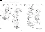
Страница 83: ...23 Exploded Views 23 1 Cabinet Parts Location SA PM33EE 83 ...

Страница 84: ...23 2 Cassette Deck RAA4402 1S Traverse Deck Part Location SA PM33EE 84 ...

Страница 85: ...23 3 Packaging SA PM33EE 85 ...

Страница 86: ...SA PM33EE 86 ...

Страница 87: ...1 1 BRAKE ROD M 121 RMM0133 1 EJECT ROD M 122 RMQ0519 REEL HUB M 123 RMS0398 1 MOVING CORE M 124 RXQ0470 2 PLUNGER M 125 RMC0061 PACK SPRING M 126 RXF0061 1 FLYWHEEL F ASS Y M 128 RXG0040 FF RELAY GEAR ASS Y M 129 RMK0283A 2 SUB CHASSIS M 130 RXL0124 PINCH ROLLER F ASS Y M 130 1 RMB0401 PINCH ARM SPRING F M 132 RXL0126 WINDING ARM ASS Y M 133 RXQ0412 3 HEAD PANEL ASS Y M 133 1 RMB0405 1 FR ROD SPR...

Страница 88: ...5948FPE2 IC 4 CH DRIVE M TRANSISTORS Ref No Part No Part Name Description Remarks Q221 B1ABGC000001 TRANSISTOR M Q222 B1ABGC000001 TRANSISTOR M Q421 B1ABGC000001 TRANSISTOR M Q422 B1ABGC000001 TRANSISTOR M Q500 B1GCCFGA0006 TRANSISTOR M Q501 B1AACF000063 TRANSISTOR M Q503 B1BCCG000002 TRANSISTOR M Q504 B1AACF000063 TRANSISTOR M Q505 B1AAJC000019 TRANSISTOR M Q507 B1AAJC000019 TRANSISTOR M Q530 2SD...

Страница 89: ...204 G0C3R3JA0027 COIL M L300 G0AR76Y00002 CHOKE COIL M L301 G0AR76Y00002 CHOKE COIL M L302 G0AR76Y00002 CHOKE COIL M L303 G0AR76Y00002 CHOKE COIL M L600 G0B371HA0005 LINE FILTER M L801 J0JKB0000020 EMI BEAD CORE M L802 J0JKB0000020 EMI BEAD CORE M L803 J0JKB0000020 EMI BEAD CORE M L804 G0C3R3JA0027 COIL M L805 G0C3R3JA0027 COIL M L806 G0A200D00002 RF CHOKE COIL M Ref No Part No Part Name Descripti...

Страница 90: ...Part No Part Name Description Remarks R223 ERJ6GEYJ470V 47 1 10W M R224 ERJ3GEYJ102V 1K 1 16W M R225 ERJ6GEYJ470V 47 1 10W M R226 D0GB392JA007 3 9K 1 16W M R227 D0GB392JA007 3 9K 1 16W M R230 D0GB104JA007 100K 1 16W M R251 ERDS2TJ821T 820 1 4W M R256 D0AE563JA048 56K 1 4W M R285 ERDS2TJ822T 8 2K 1 4W M R291 ERDS2TJ682T 6 8K 1 4W M R292 D0AE332JA048 3 3K 1 4W M R295 ERDS2TJ681T 680 1 4W M R380 D0AE...

Страница 91: ...1 16W M R879 D0GB104JA007 100K 1 16W M R880 D0GB472JA041 4 7K 1 16W M Ref No Part No Part Name Description Remarks R882 ERJ3GEYJ102V 1K 1 16W M R883 D0GB103JA007 10K 1 16W M R885 D0GB104JA007 100K 1 16W M R886 ERJ3GEYJ102V 1K 1 16W M R887 ERJ3GEYJ102V 1K 1 16W M R888 ERJ3GEYJ102V 1K 1 16W M R889 D0GB101JA007 100 1 16W M R890 D0GB153JA007 15K 1 16W M R891 D0GB153JA007 15K 1 16W M R892 D0GB104JA007 ...

Страница 92: ...F1D1H1040002 0 1 50V M C372 F1D1H102A012 1000P 50V M C373 F1D1H471A012 470P 50V M C374 ECA1HAK100XB 10 50V M Ref No Part No Part Name Description Remarks C375 F1H1H102A219 1000P 50V M C376 ECQV1H224JL3 0 22 50V M C401 F1H1H221A748 220P 50V M C403 F1H1H221A748 220P 50V M C405 F1H1H221A748 220P 50V M C409 F1H1H102A219 1000P 50V M C410 F1H1H221A748 220P 50V M C411 F1H1H102A219 1000P 50V M C412 ECJ1VB...

Страница 93: ...10 F1H1H682A219 6800P 50V M C1121 F1H1H102A219 1000P 50V M Ref No Part No Part Name Description Remarks C1122 F1H1H103A219 0 01 50V M C1123 ECJ1VB1H271K 270P 50V M C1201 ECA1HAK010XB 1 50V M C1202 F1H1H471A219 470P 50V M C1203 ECA1CAK101XB 100 16V M C1204 F1H1C2730001 0 027 16V M C1205 F1H1H471A219 470P 50V M C1206 ECA1HAK2R2XB 2 2 50V M C1207 F1H1H152A219 1500P 50V M C1208 F2A1C1000018 10P 16V M ...

Страница 94: ...Description Remarks C7352 ECJ1VB1C183K 0 018 16V M C7601 ECEA0JKA330I 33 6 3V M C7613 F1H1C104A041 0 1 16V M C7614 F2A0J101A198 100P 6 3V M C7626 F1H1C104A041 0 1 16V M C7670 F1H1C104A041 0 1 16V M 94 SA PM33EE FLE0603A J M S P ...

Отзывы: