- 31 -
Service Manual
Service Mode (Electronic Controls, Continued)
Red, Green & Blue Screen Cutoff
1.
Use either a no input signal condition or raster from
the NTSC generator.
2.
Observing the green tube directly or via a reflective
surface, adjust the VR on focus pack for the green
tube for minimum noise.
3.
Adjust the noise level in the red and blue tubes to
match the noise level in the green tube.
White Balance Adjustment
Prior to this adjustment, perform Contrast adjustment.
This adjustment requires that the service use skills in
observing what a screen without color should look like
(White Picture).
1.
Enter the service mode.
2.
Apply a black and white pattern to one of the video
inputs.
High Light White Balance Adjustment
1.
Adjust DAC R_DR for Red and B_DR for Blue
adjustments.
2.
Make sure the screen is not blue or Green. The
screen should be white in all areas.
3.
Check the black and white pattern for a black and
white picture with even shades of gray and no color
tint in the picture.
Low Light White Balance Adjustment
1.
Adjust DAC CUT_R for Red and DAC CUT_B for
Blue.
2.
Check the screen for even white in all areas, no
color.
3.
Check the black and white pattern for a black and
white picture, even shades of gray and no color tint
in the low light areas.
4.
Repeat the High Light and Low Light White
Balance again until the white balance tracks from
high light to low light.
Tint and Color Check
Again, the service ability to see color and the balance
of color is important for theses adjustments.
Tint Check
1.
In Picture Menu set Picture Norm to YES.
2.
Apply color bars to the video input.
3.
Magenta is composed of two colors, blue and red.
4.
Check to see that magenta does not have too
much blue or too much red.
5.
Check cyan. Cyan is composed of blue and green.
It should not have too much blue or green.
6.
Use a test signal from a VCR or laser disk that has
a pre-recorded close up of a signal that has good
flesh tones.
7.
The signal on the VCR or laser disk should look
normal.
Color Check
Using a clean RF or video signal, set the color level so
that it does not saturate or appear harsh. Make sure
that color is not set so that it appears dull and washed
out. Look for natural colors, try to adjust the picture to
appear as a normal photograph.
MTS Circuit Adjustments
Note: It is important to adjust the MTS circuit in the
order shown below.
The MTS Circuit Adjustments require two steps:
1.
Input Level Adjustment.
2.
Stereo Separation Adjustment.
Input Level Adjustment (MTSIN)
Preparation:
1.
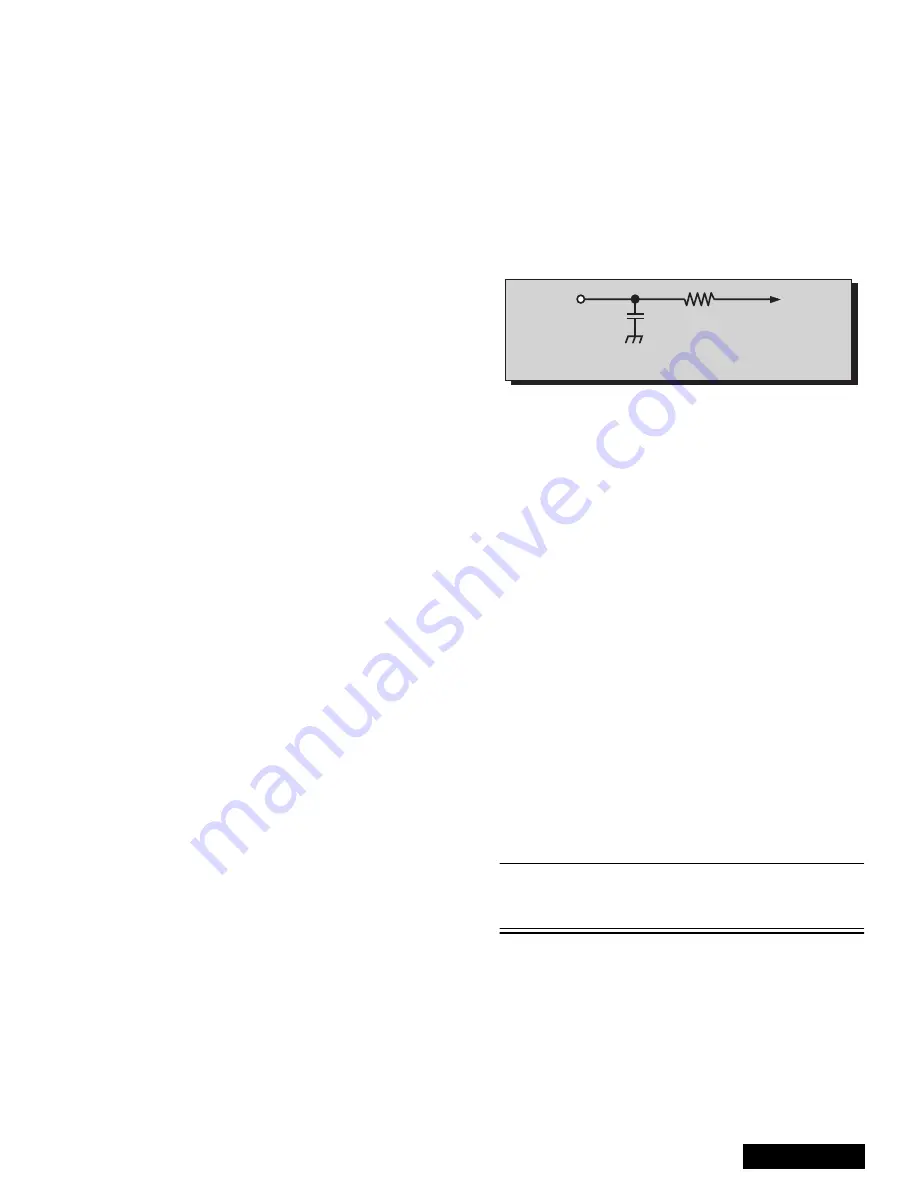
Connect an RMS meter (AC Range) with filter jig
as shown in Figur e60.
2.
Connect an RF signal generator to the RF
antenna input.
Procedure:
1.
Apply the following signal from the RF signal
generator:
Video: 100 IRE flat field, 30% modulation.
Audio: 300Hz, 100% modulation, monaural
(70 ± 5dB, 75
Ω
OPEN, P/S 10dB). Make sure to
turn off 75
µ
s pre-emphasis.
2.
Adjust (MTSIN)
MTS-INPUT
data until the voltage
measured is 106mV ± 6.0mV rms.
Stereo Separation Adjustment
(SEPAL & SEPAH)
Preparation:
1. Connect an RF signal generator to the RF
antenna input.
2.
Connect an oscilloscope probe to TPE10 (R_out).
Procedure:
1.
Set PTV to Stereo Mode (in the Audio Menu).
2.
Apply the following signal from the RF signal
generator:
Video: 100 IRE flat field, 30% modulation.
Audio: 300Hz, 30% modulation, stereo (left only)
(70dB ± 5dB, 75
Ω
OPEN, P/S 10dB).
Note: Set the 30% modulation with the pilot
light SW and N.R. switches OFF then turn
them ON while testing.
3.
Adjust MTS Low-Level Separation (SEPAL) data
(in the Service Adjustment Menu)
until the amplitude
of the measured waveform on the scope
is minimum.
4.
Apply the following signal from the RF
signal generator:
Video: 100 IRE flat field, 30% modulation.Audio:
3KHz, 30% modulation, stereo (left only).
(70dB ± 5dB, 75
Ω
OPEN, P/S 10dB).
10k
4700p
Figure 60. Filter Jig
TPE11
RMS
METER
L_OUT
Содержание PT- 65WX51E
Страница 25: ... 25 Service Manual G Board K Board Schematics G Board Schematic K Board Schematic ...
Страница 26: ... 26 Service Manual G Board K Board PCB G Board PCB K Board PCB ...
Страница 27: ... 27 Notes ...
Страница 28: ... 28 Printed in USA K01062205PL0627 ...
Страница 56: ... 28 A BOARD SCHEMATIC DIAGRAMA ELÉCTRICO TARJETA A A BOARD TARJETA A ...
Страница 57: ... 29 A BOARD SCHEMATIC DIAGRAMA ELÉCTRICO TARJETA A A BOARD TARJETA A ...
Страница 58: ... 30 A BOARD SCHEMATIC DIAGRAMA ELÉCTRICO TARJETA A A BOARD TARJETA A ...
Страница 59: ... 31 A BOARD SCHEMATIC DIAGRAMA ELÉCTRICO TARJETA A A BOARD TARJETA A ...
Страница 61: ... 33 Notes ...
Страница 62: ... 34 Printed in USA K01052203ZR0511 ...
Страница 111: ... 49 ALL MODELS D Board Layout ...
Страница 112: ... 50 ALL MODELS D Board Schematic Left Portion ...
Страница 113: ... 51 ALL MODELS D Board Schematic Right Portion ...
Страница 114: ... 52 ALL MODELS A Board Schematic Left Portion ...
Страница 115: ... 53 ALL MODELS A Board Schematic Left Middle Portion ...
Страница 116: ... 54 ALL MODELS A Board Schematic Right Middle Portion ...
Страница 117: ... 55 ALL MODELS A Board Schematic Right Portion ...
Страница 118: ... 56 ALL MODELS DH Board Schematic ...
Страница 125: ... 63 Notes ...
Страница 126: ... 64 Printed in USA K01052205PL0518 ...


