- 7 -
Service Manual
Service notes
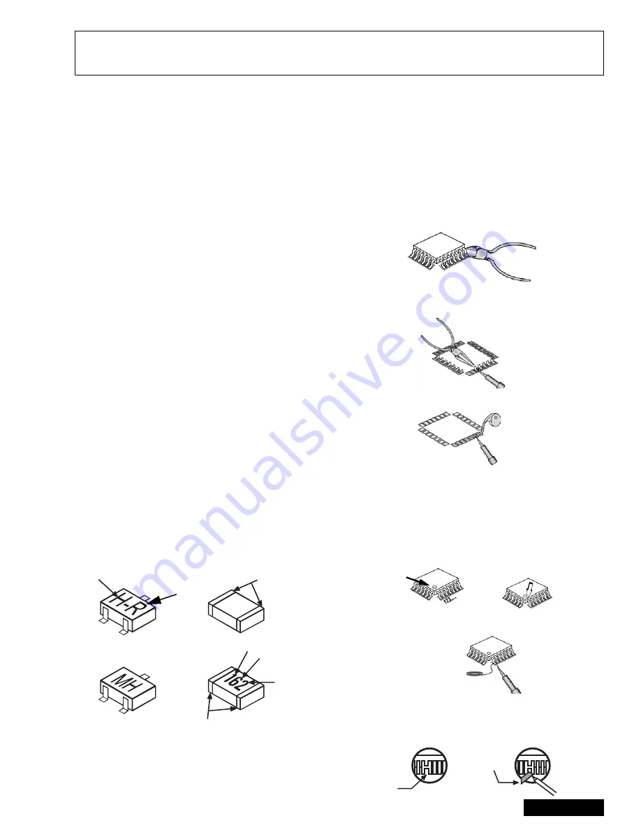
Leadless chip component
(surface mount)
Chip components must be replaced with identical chips
due to critical foil track spacing. There are no holes in
the board to mount standard transistors or diodes.
Some chip capacitor or resistor board solder pads may
have holes through the board, however the hole
diameter limits standard resistor replacement to 1/8
watt. Standard capacitor may also be limited for the
same
reason.
It
is
recommended
that
identical
components be used.
Chip resistor have a three digit numerical resistance
code - 1st and 2nd significant digits and a multiplier.
Example: 162 = 1600 or 1.6k
Ω
resistor, 0 = 0
Ω
(jumper).
Chip capacitors generally do not have the value
indicated on the capacitor. The color on the component
indicates the general range of the capacitance.
Chip transistors are identified by a two letter code. The
first letter indicated the type and the second letter, the
grade of transistor.
Chip diodes have a two letter identification code as per
the code chart and are a dual diode pack with either
common anode or common cathode. Check the parts
list for correct diode number.
Component removal
1.
Use solder wick to remove solder from component
end caps or terminal.
2.
Without pulling up, carefully twist the component
with tweezers to break the adhesive.
3.
Do
not
reuse
removed
leadless
or
chip
components since they are subject to stress
fracture during removal.
Chip component installation
1.
Put a small amount of solder on the board
soldering pads.
2.
Hold the chip component against the soldering
pads with tweezers or with a miniature alligator clip
and apply heat to the pad area with a 30 watts iron
until solder flows. Do not apply heat for more than
3 seconds.
How to replace Flat-IC
- Required tools -
1.
Cut the pins of the defective IC with the wire cutter
pliers, and remove it completely away from the
board. If the IC is glued to the board, apply hot air
to complete the removal. CAUTION- Do not pull or
twist the pliers, it may damage the soldering pads
in the board .
2.
Using the soldering Iron and the long nose pliers,
remove the IC pins that are still attached to the
board.
3.
Using the de-solder braid and the soldering Iron,
remove the solder from the board soldering pads.
4.
Position the new flat IC in place (apply the pins of
the flat IC to the soldering pads where the pins
need to be soldered). Properly determine the
positions of the soldering pads and pins by
correctly aligning the polarity symbol. Start aligning
and soldering Pin No.1, then align and solder the
pin in the apposite corner of the IC, this will help to
align the rest of the pins.
5.
Solder all pins to the soldering pads using a fine
tipped soldering iron.
6.
Check with a magnifier for solder bridge between
the pins or for dry joint between pins and soldering
pads. To remove a solder bridge, use a de-solder
braid as shown in the figure below.
Note: These components are affixed with glue. Be careful not to break or damage any foil under the
component or at the pins of the ICs when removing. Usually applying heat to the component for
a short time while twisting with tweezers will break the component loose.
c
b
e
Chip components
TRANSISTOR
CAPACITOR
RESISTOR
MH DIODE
SOLDER
CAPS
SOLDER
CAPS
1ST DIGIT
2ND DIGIT
MULTIPLIER
=1600 = 1.6k
GRADE
TYPE
COMMON
ANODES
CATHODE
c
b
e
•
Soldering iron
•
De-solder braids
•
Sharp pliers (wire
cutters and long nose)
•
Magnifier
Flat-IC
Soldering
Iron
De-Solder
Braid
Soldering
Iron
Polarity
symbol
Soldering
Iron
Solder
De-Solder
Braid
Solder
Bridge
Soldering
Iron
Содержание PT-47WX42CF
Страница 65: ... 65 Notes PARTS LIST ...
Страница 66: ... 66 D Board Schematic ...
Страница 67: ... 67 D Board Schematic ...
Страница 68: ... 68 D Board Schematic ...
Страница 69: ... 69 Jumper between pin 7 and pin 1 D Board Schematic ...
Страница 70: ... 70 D Board Schematic ...
Страница 71: ... 71 D Board Schematic ...
Страница 73: ... 73 NOTES NOTES ...
Страница 74: ... 74 D Board Layout ...
Страница 75: ... 75 D Board Layout ...
Страница 76: ... 76 A Board Schematic ...
Страница 77: ... 77 A Board Schematic ...
Страница 78: ... 78 A Board Schematic ...
Страница 79: ... 79 A Board Schematic ...
Страница 80: ... 80 A Board Schematic ...
Страница 81: ... 81 A Board Schematic ...
Страница 82: ... 82 A Board Schematic ...
Страница 83: ... 83 A Board Schematic ...
Страница 84: ... 84 Board section Top A Board Layout Top left portion ...
Страница 85: ... 85 Board section Top A Board Layout Top right portion ...
Страница 86: ... 86 Board section Top A Board Layout Bottom left portion ...
Страница 87: ... 87 Board section Top A Board Layout Bottom right portion ...
Страница 88: ... 88 Board section Bottom side A Board Layout Top left portion ...
Страница 89: ... 89 Board section Bottom A Board Layout Top right portion ...
Страница 90: ... 90 Board section Bottom A Board Layout Bottom left portion ...
Страница 91: ... 91 Board section Bottom A Board Layout Bottom right portion ...
Страница 92: ... 92 LG Board schematic TNP2AA112 LG Board schematic ...
Страница 94: ... 94 LR Board schematic TNP2AA111 LR Board schematic ...
Страница 96: ... 96 LB Board schematic TNP2AA110 LB Board schematic ...
Страница 98: ... 98 K Board schematic TNP2AA089 K Board layout TNP2AA089 K Board schematic and layout ...
Страница 99: ... 99 G Board schematic TNP2AA090 G Board layout TNP2AA090 G Board schematic and layout ...
Страница 104: ...Printed in USA K02042127PL0429 ...


