background image

46

KX-TGC220/KX-TGC222/KX-TGC223/KX-TGCA20

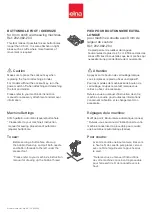
10.1.2. Handset

2 screws

ձ

Cabinet body 

Cabinet cover 

Cabinet cover 

Screw

շ

յ

Solders

Main P.C. board

2 charge terminals

ձ

Remove the 2 screws.

ղ

Insert a plastic card. 
(Ex. Used SIM card etc.) 
between the cabinet body 
and the cabinet cover, then 
pull it along the gap to open 
the cabinet.

ճ

Likewise, open the other
side of the cabinet.

մ

Remove the cabinet cover 
by pushing it upward.

յ

Remove the solders.

Remove the solders to remove
the 2 charge terminals.

ն

շ

Remove the screw to remove 
the Main P. C. board.

ն

Solders

Содержание KX-TGC220AL

Страница 1: ...KX TGC222AL KX TGC222NZ KX TGC223AL KX TGC223NZ KX TGCA20AZ Digital Cordless Answering System S Silver Version AL for Australia NZ for New Zealand Handset KX TGCA20 KX TGC220 Base Unit Charger Unit Model No Base Unit Handset Charger Unit KX TGC220 1 TGC220 1 TGCA20 KX TGC222 1 TGC220 2 TGCA20 1 KX TGC223 1 TGC220 3 TGCA20 2 KX TGCA20 1 TGCA20 1 Configuration for each model ...

Страница 2: ...c Diagrams Circuit Board Diagrams Exploded Views and Replacement Parts List It is essential that these critical parts should be replaced with manufacturer s specified parts to prevent shock fire or other hazards Do not modify the original design without permission of manufacturer IMPORTANT INFORMATION ABOUT LEAD FREE PbF SOLDERING If lead free solder was used in the manufacture of this product the...

Страница 3: ...tion 37 9 1 11 Check Caller ID 37 9 1 12 Bell Reception 38 9 1 13 Check TAM Operation 38 9 2 Troubleshooting by Symptom Base Unit and Charger Unit 39 9 2 1 Check Point Base Unit 39 9 3 Troubleshooting by Symptom Handset 41 9 3 1 Check Point Handset 41 10 Disassembly and Assembly Instructions 44 10 1 Disassembly Instructions 44 10 1 1 Base Unit 44 10 1 2 Handset 46 10 1 3 Charger Unit 47 10 2 How t...

Страница 4: ...ew and Replacement Parts List 79 15 1 Cabinet and Electrical Parts Base Unit 79 15 1 1 KX TGC220 79 15 2 Cabinet and Electrical Parts Handset 80 15 3 Cabinet and Electrical Parts Charger Unit 81 15 4 Accessories 82 15 5 Replacement Parts List 83 15 5 1 Base Unit 83 15 5 2 Handset 84 15 5 3 Charger Unit 85 15 5 4 Accessories and Packing Materials 85 15 5 5 Screws 86 15 5 6 Fixtures and Tools 86 ...

Страница 5: ... of used batteries according to the manufacture s Instructions 2 2 About Lead Free Solder PbF Pb free Note In the information below Pb the symbol for lead in the periodic table of elements will refer to standard solder or solder that contains lead We will use PbF solder when discussing the lead free solder used in our manufacturing process which is made from Tin Sn Silver Ag and Copper Cu This mod...

Страница 6: ...Bi Please check the manufacturer s specific instructions for the melting points of their products and any precautions for using their product with other materials The following lead free PbF solder wire sizes are recommended for service of this product 0 3 mm 0 6 mm and 1 0 mm 2 3 Discarding of P C Board When discarding P C Board delete all personal information such as telephone directory and call...

Страница 7: ...tiple Access Channel Spacing 1 728 kHz Bit Rate 1 152 kbit s Modulation GFSK Gaussian Frequency Shift Keying RF Transmission Power Approx 10mW average power per channel Voice Coding ADPCM 32 kbit s Operating conditions 0 C 40 C 20 80 relative air humidity dry Power source AC Adaptor 220 240 V AC 50 60 Hz Base unit PNLV226AL0Z Charger PNLV233ALKZ Power consumption Base unit Standby Approx 0 54 W Ma...

Страница 8: ...Q161 Q141 BELL DETECT HOOK BELL Q111 LIN LOUT RF_PART HSMIP HSMIN IC501 BBIC INUSE DETECT 2 INUSE DETECT 1 RECEIVE AMP DCIN 1 DCIN 2 IC302 VCCPA VBAT_APU VBAT VCC_FE VCC_IF VCC_VCO 3 0V DOUBOUT SCL SDA WP VDD ANS_LED IC601 FLASH MEMORY IC611 EEPROM MEMORY KEYS R151 R152 R131 R133 Q171 VBAT DL CS MSG_LED KEY 1 3 KEY C D E SPOUTN SPOUTP 3 0 V REGULATOR CLK DO STM CKM R371 R372 VCCA VCC XIN XOUT RXp ...

Страница 9: ...cellation and Echo suppression DSP section Any tones tone sidetone ringing tone etc generation DSP section DTMF receiver DSP section Clock Generation for RF Module ADC DAC timer and power control circuitry PLL Oscillator Detector Compress Expander First Mixer All interfaces ex QSPI FLASH MEMORY EEPROM LED Analog Front End etc Integrated 1 9GHz PA for DECT EEPROM IC611 Temporary operating parameter...

Страница 10: ...10 KX TGC220 KX TGC222 KX TGC223 KX TGCA20 4 3 Block Diagram Base Unit_RF Part RXp RXn ANT1 TXp TXn ...

Страница 11: ...rded message The BBIC implements synthesized Voice utilizing the built in speech detector and a Flash Memory which stored the vocabulary Caller ID demodulation The BBIC implements monitor and demodulate the FSK DTMF signals that provide CID information from the Central Office Digital Switching The voice signal from telephone line is transmitted to the handset or the voice signal from the handset i...

Страница 12: ... and analog part is insulated from VBAT by Doubler of BBIC Circuit Operation 5 5V VBAT RSTN Reset pin 54 VBAT pin 10 pin 57 pin 9 pin 15 IC501 IC302 IC601 BBIC DOUBLER OUT For peripherals VDDC 1 2V AC Adaptor 3 0V REGULATOR FLASH IC611 EEPROM 3 0V STM CKM Receive Amp RF Part ANS LED MSG LED Startmonitor IC501 57pin VDDC 1 2 V VBAT Reset RSTN IC501_54 pin BBIC chip initialize CKM STM ...

Страница 13: ...13 KX TGC220 KX TGC222 KX TGC223 KX TGCA20 4 4 4 1 Charge Circuit The voltage from the AC adaptor is supplied to the charge circuits D361 R372 R371 F301 DCP 5 5V CHARGE CHARGE DCM D362 C351 ...

Страница 14: ...111 Q111 BBIC pin 5 BELL When the CPU BBIC detects a ring signal Q141 turns on thus providing an off hook condition active DC current flow through the circuit Following signal flow is the DC current flow T D101 Q141 Q161 R163 D101 P101 R ON HOOK Circuit Q141 is open Q141 is connected as to cut the DC loop current and to cut the voice signal The unit is consequently in an on hook condition Pulse Di...

Страница 15: ... Analog Front End D A A D 35 37 21 22 17 18 34 33 66 67 32 24 44 45 73 63 64 77 76 ADPCM Codec Filter DSP Speech Decoding Speech Encoding BMC Burst Decoding ANT1 Burst Encoding RF PLL MOD DEMOD 1 2 87 86 RXn ANT1 RXp TXp TXn 7 8 XTAL X1 10 368 MHz BATTERY 46 ON SWITCH KEYPAD Charge Pump ROWS COLUMNS CP3V CP4V 57 58 59 60 11 12 13 14 25 55 47 48 51 53 QSPI IO 0 3 BBIC IC1 IC7 65 LCD BACK LIGHT KEY ...

Страница 16: ... Charge Circuit Circuit Operation When charging the handset on the Base Unit the charge current is as follows DC 5 5 V R371 R372 D362 CHARGE Base CHARGE Handset Q3 BATTERY Battery BATTERY R45 GND CHARGE Handset CHARGE Base GND DC GND In this way the BBIC on Handset detects the fact that the battery is charged The charge current is controlled by switching Q9 of Handset Refer to Fig 101 in Power Sup...

Страница 17: ... D101 Q141 R165 R177 C173 Q171 C178 R178 IC501 16 73 74 IC601 IC601 IC501 73 74 29 31 SPEAKER IC501 28 C184 Q161 Q141 D101 P101 T R TEL LINE T R TEL LINE P101 C121 C122 R121 R122 IC501 24 25 T R TEL LINE P101 R111 R112 C111 C112 Q111 IC501 5 HANDSET TX HANDSET RX HANDSET SP Phone TX HANDSET SP Phone RX SIGNAL ROUTE IN 䊻㻌 ROUTE 䊻㻌 OUT GREETING RECORDING GREETING PLAY TO TEL LINE ICM RECORDING ICM P...

Страница 18: ...0 RF part signal route SIGNAL ROUTE IN 䊻㻌 ROUTE 䊻㻌 OUT HANDSET RF TX_ROUTE HANDSET RF RX_ROUTE BASE UNIT RF TX_ROUTE BASE UNIT RF RX_ROUTE IC1 86 87 C859 ANT ANT IC 1 2 IC501 44 45 C819 C872 ANT ANT C872 C895 IC501 46 47 Note inside of Handset ...

Страница 19: ...rating Instructions Instruction book on TSN Server 7 1 For Service Hint right soft key 132 Items Contents Battery You could use other rechargeable batteries sold in a market but the unit is not guaranteed to work properly The battery strength may not be indicated correctly if the battery is disconnected and connected again even after it is fully charged In that case by recharging the battery as me...

Страница 20: ...eration V 4 Enter 7 2 6 2 7 6 6 4 Note 7262 7664 PANA SONI see letters printed on dial keys 6 Enter Address 1 7 Enter New Data 1 5 Select Write EEP using or then press or V 3 Select Line Setup using or then press OK or V _ _ _ _ _ _ H S LCD Set Addr Default Data Set Addr C OK New Data Set Addr C OK 8 Press a long confirmation beep will be heard OK OK Service Mode Read EEP Write EEP OK TALK Talk So...

Страница 21: ...5 08 00 0B 4C 3 dB up 0F F6 6 dB up When hex changes from 00 01 to 0B 4C or 0F F6 gain increases by 3 dB or 6 dB Frequency 00 08 00 07 01 00 Use these items in a READ ONLY mode to confirm the contents Careless rewriting may cause serious damage to the computer system ID 00 02 00 06 Given value Bell length 03 C6 32 5 sec 2 1E 3 sec 14 2 sec This is time until bell stops ringing Unit 100 msec Desire...

Страница 22: ...s OK H S key operation V 3 Enter 7 2 6 2 7 6 6 4 Note 7262 7664 PANA SONI see letters printed on dial keys 6 Enter Address 1 7 Enter New Data 1 4 Select Write EEP using or then press or V _ _ _ _ _ _ H S LCD Set Addr Default Data Set Addr C OK New Data Set Addr C OK 8 Press a long confirmation beep will be heard OK OK Service Mode Read EEP Write EEP OK ECO Dial keypad TALK Talk Soft keys Volume ke...

Страница 23: ...ng may cause serious damage to the handset Items Address Default Data New Data Possible Adjusted Value MAX hex Possible Adjusted Value MIN hex Remarks Battery Low 00 09 70 2 Frequency 00 07 00 08 70 02 ID 00 02 00 06 Given value Desired Number hex Input Keys Desired Number hex Input Keys 0 0 A R 0 1 1 B R 1 C R 2 D R 3 E R 4 9 9 F R 5 Item Default Data New Data Destination E7 EB E3 Sending level 3...

Страница 24: ...zed by only F command 0 The data initialized by F and 0 command 1 The data initialized by F 0 and 1 command 2 The data initialized by F 0 1 and 2 command 3 The data initialized by all command F 0 1 2 3 Country Setting Description x Default no specific country setting so revert to default value Address Initial Type Name Description Default value Country Setting 04 B0 3 EEP_Language Selected Languag...

Страница 25: ...istration to the base unit is cancelled If the handset needs to be registered to the base unit refer to Registering a Handset to a Base Unit in the Operating Instructions If users do not bring the base unit with them the registration procedure has to be done by users themselves 1 Connect the AC adaptor to the base unit and install the charged batteries into the handset 2 Confirm the handset is reg...

Страница 26: ... P 37 Check Caller ID P 37 Power ON Base Unit OK FLOW CHART Check Power OK Playback Pre Message Check Playback Record OK Check Record Range Check the RF part Handset Voice Transmission Check Handset Transmission Handset Voice Reception OK OK OK Check Handset Reception Caller ID Reception Check Caller ID Caller ID Error No voice No voice No charge Not playback Not record Not working NG No link OK L...

Страница 27: ...ES Check AC Adaptor Check VDDC 1 2 V Test Point VDDC OK Check Power Supply Circuit NO NO NO NO RSTN Reset High YES Check Reset Circuit Check Xtal CLK 13 824 MHz YES Check X501 Check BBIC Check Power Supply Circuit Reset Circuit Check BBIC IC1 Check F1 is not open Check X1 Is the voltage of BATT 2 3 V more Check the battery and around BATT and BATT are not shorted Is the battery inserted BATT and B...

Страница 28: ...erface P 14 Note Flash Memory is IC601 BBIC is IC501 Check Bell signal OK Check Telephone Line Interface Bell Does the unit catch line YES Check Telephone Line Interface OFF HOOK Check Line In Pin 16 of BBIC Check ICM Recording in Signal Route NO OK Check Auto Disconnect Circuit OK Check Parallel Connection Detection Circuit OK Check BBIC and Flash Memory NO NO ...

Страница 29: ... output of BBIC Pin 29 31 OK Check BBIC and Flash Memory Check Speaker and its surroundings NO NO Check Charge Circuit of Base Unit Check Handset Plug in the AC Power source Charge Handset on Base Unit Is the voltage of two charge contacts about 3 V or more OK NO Check Charge Contacts at Base Unit from mechanical point of view YES Is BBIC IC1 34 high at charge state Check Charge Circuit Check Powe...

Страница 30: ...then check the TP_CKM IC501 57pin To adjust frequency send command SFR until the frequency counter becomes13 824 MHZ 55HZ Check around Power Supply Circuit Adjust 3 0V voltage to 3 0 V Does Base Unit make link with normal working Handset Check around X501 and RF module and adjust clock frequency NO NO NO NO YES YES Is the voltage of VBAT about 3 0 V Check the RF part Does the RF clock CLK oscillat...

Страница 31: ...to Do after Replacing IC or X tal P 56 for Handset Check around Power Supply Circuit Reset Circuit Check BBIC IC1 Does Handset make link with Base Unit Correct working unit Check around X1 and adjust clock frequency NO NO NO NO Is the voltage of 1 8V about 1 8 V YES YES YES YES Is the voltage of CP3V about 3 0 V Does the RF clock CLK oscillate 10 368 MHz in Handset Test Mode YES Is the voltage of ...

Страница 32: ...2 2 a Re register regular HS Normal mode to base unit to be checked If this operation fails in some ways the base unit is defective b Re register handset to be checked to regular BU Normal mode If this operation fails in some ways the handset is defective Base unit is defective Handset is defective START Registration of Regular HS to base unit Registration of handset to Regular BU other checkings ...

Страница 33: ...e each item Note 1 Refer to Check Link P 30 Start Link confirmation Normal 1 Control signal confirmation X tal Frequency confirmation TX confirmation RX confirmation Range confirmation Normal TEST RANGE Check Check BBIC interface parts RF Block BBIC on BU HS P C B Adjust X tal Frequency 1 Check TX Block Check RX Block GOOD 6 2 3 4 5 OK OK OK OK NG NG NG NG NG NG OK OK ...

Страница 34: ...d RXDATA waveform of Regular HS by Digital Oscilloscope 1 Place Regular BU 15 cm away from a checked HS 2 Confirm TXDATA waveform of HS 2 and RXDATA waveform of Regular BU by Digital Oscilloscope 4 RX confirmation Regular HS BU Mode Test TX_Burst Mode BU HS Mode Test RX Mode 1 Place Regular HS 15 cm away from a checked BU 2 Confirm RXDATA waveform of BU 1 and TXDATA waveform of Regular HS by Digit...

Страница 35: ...distance of about 20m between HS and BU Link OK TX Power of the HS is OK No Link TX Power of the HS is NG Range Confirmation RX TEST RX sensitivity check HS BU setting Checked unit High TX power 1 Regular unit Low TX power 1 1 Register Regular HS to BU to be checked 2 Set TX Power of the BU and the Regular HS according to CHART1 3 At distance of about 20m between HS and BU Link OK RX Sensitivity o...

Страница 36: ...bout 5 seconds L If all registered handsets start ringing press LOCATOR again to stop then repeat this step KX TGC222 KX TGC223 L The next step must be completed within 90 seconds 3 Handset Press OK then wait until a long beep sounds 1 3 0 1 MENU 2 All handsets registered to the base unit are displayed L 3 1 3 1 Select the handset you want to cancel V i OK Yes V i OK i OFF ...

Страница 37: ...face P 14 Note Make sure the format of the Caller ID service of the Telephone company that the customer subscribes to It is also recommended to confirm that the customer is really a subscriber of the service Check MIC of handset Check handset Tx in Signal Route Check speaker of handset Check handset Rx in Signal Route YES Did bell ring Message indicator blinks Check Calling Line Identification Cal...

Страница 38: ...R477 R478 YES Check around C103 C104 C105 C106 C107 C109 C110 C111 C113 R101 R102 R103 R104 R109 R110 R111 R112 P101 NO When bell signal is coming is there bell sound signal at IC501 SPP SPN 1 Does the bell sound from SPEAKER Check around SP SP When bell signal coming is there bell sound signal at BBIC IC1 35 37 NO NO YES When bell signal coming is there bell sound signal at SP SP YES Check BBIC I...

Страница 39: ... the voltage between test point VDD1 and GND is 1 8 V 0 02 V 2 Execute the command VDD then check the current value 3 Adjust the 1 8V voltage of VDD1 executing command VDD XX XX is the value Q301 IC501 R311 C311 C516 C517 C Charge Pump 3 0V Supply Confirmation VDD5 1 Confirm that the voltage between test point VDD5 and GND is 3 0 V 0 1 0 3 V IC501 C512 D Charge Pump 3 0V Supply Confirmation VDD4 1...

Страница 40: ...er to J M Sensitivity Receiver Confirmation ANTI_TP Follow steps 1 to 6 of J 7 Set DECT tester power to 88 dBm 8 Confirm that the BER is 1000 ppm Refer to J N Power RAMP Confirmation Follow steps 1 to 6 of J 7 Confirm that Power RAMP is matching Refer to J O Audio Check 1 Link with Handset which is connected to Line Simulator 2 Set line voltage to 48 V and line current to 50 mA 3 Input 45 dBm 600 ...

Страница 41: ...tem O Check item O Items Check Point Procedure Check or Replace Parts A 1 8 V Supply Adjustment 1 8V 1 Confirm that the voltage between test point 1 8V and GND is 1 8 V 0 02 V 2 Execute the command VDD then check the current value 3 Adjust the 1 8V voltage of 1 8V executing command VDD XX XX is the value IC1 Q1 C44 R45 C40 C45 B BBIC Confirmation 1 BBIC Confirmation Execute the command getchk 2 Co...

Страница 42: ...it after measurement IC1 X1 C47 I Transmitted Power Confirmation Short Antenna pattern to GND 1 Configure the DECT tester CMD60 as follows Setting Test mode PP RFPI 0102030405 Traffic Carrier 5 Traffic Slot 4 Mode Loopback RF LEVEL 70 dBm PACKET PP32Z 2 Execute the command sendchar TST 01 02 03 04 05 3 Initiate connection from DECT tester 4 Confirm that the NTP value at ANT is 19 dBm 25 dBm IC1 C8...

Страница 43: ...SP and SP 5 Confirm that the level is 10 0 dBm 3 dB for NZ or 9 0 3 dBm for AL and that the distortion level is 5 vol Max at SP 8 Load IC1 C78 C79 R76 R77 P Charge Pump 3 0 V Supply Confirmation CP3V 1 Confirm that the voltage between testpoint CP3 0V and GND is 3 0 V 0 3 V C30 C53 C29 Q Charge Pump CP4V Supply Confirmation CP4V 1 Confirm that the voltage between testpoint CP4V and GND is 4 0 V 0 ...

Страница 44: ... 10 Disassembly and Assembly Instructions 10 1 Disassembly Instructions 10 1 1 Base Unit 10 1 1 1 KX TGC220 ձ Remove the 2 screws to remove the cabinet cover ղ Remove the solders ճ Remove the main P C board ճ Main P C board ձ 4 screws Solders ղ ...

Страница 45: ...45 KX TGC220 KX TGC222 KX TGC223 KX TGCA20 մ Remove the 2 screws to remove the charge case and the operational P C board Operational P C board Chage case մ Screw մ Screw ...

Страница 46: ... 2 screws ղ Insert a plastic card Ex Used SIM card etc between the cabinet body and the cabinet cover then pull it along the gap to open the cabinet ճ Likewise open the other side of the cabinet մ Remove the cabinet cover by pushing it upward յ Remove the solders Remove the solders to remove the 2 charge terminals ն շ Remove the screw to remove the Main P C board ն Solders ...

Страница 47: ...47 KX TGC220 KX TGC222 KX TGC223 KX TGCA20 10 1 3 Charger Unit ձ ղ Remove the solders to remove the 2 charge terminals 2 charge terminals Remove the cabinet cover ղ Solders ձ Cabinet Cover ...

Страница 48: ... not damaged Fit the heatseal of a new LCD Rubber of Soldering Iron Part No PQZZ430PRB Tip of Soldering Iron Part No PQZZ430PIR Heatweld with the tip of the soldering iron about 5 to 8 seconds in case of 60W soldering iron New LCD 0 2 mm 0 2 mm P C board If interval tolerance between center lines is less than 0 2 mm it is o k Horizontal Interval Tolerance Vertical Interval Tolerance OK NG NG NG Ho...

Страница 49: ...tion 11 2 The Setting Method of JIG Preparation Serial JIG cable PQZZ1CD300E PC which runs in DOS mode Batch file CD ROM for setting Refer to parts list of Fixtures and Tools P 86 Note If you have the JIG Cable for TCD500 series PQZZ1CD505E change the following values of resistance Then you can use it as a JIG Cable for both TCD300 and TCD500 series It is an upper compatible JIG Cable 11 2 1 Conne...

Страница 50: ...ow 3 At the DOS prompt type D for example to select the drive then press the Enter key 4 Type CD 㪳PNZZTG then press the Enter key 5 Type SET_COM X then press the Enter key X COM port number used for the serial connection on your PC 6 Type READID then press the Enter key 䊶If any error messages appear change the port number or 䇭check the cable connection 䊶If any value appear go to next step 7 Type D...

Страница 51: ...DCM DCP C601 3 0V SA101 C611 CHARGE F301 CHARGE ANT1 TCK UGND ANT1_Short URX TDI UTX STM CKM P15 IC601 IC611 R111 Q171 R 1 1 2 R113 R114 R321 R322 C112 C113 TMS VDDC L1R L1T C120 R164 C513 C321 C515 R171 R172 5 5V R175 RA611 R176 R371 R372 C342 C351 C167 C171 D113 C175 C176 C178 VREF IC302 ANT1_S GND C115 R115 C193 R177 R158 R165 R149 R148 Q140 SA102 R104 GAP R103 R117 C110 C104 C103 R118 R 1 1 6 ...

Страница 52: ...ge the following values of resistance Then you can use it as a JIG Cable for both TCD300 and TCD500 series It is an upper compatible JIG Cable 11 4 1 Connections Connect the DC Power or Battery to BATT and BATT Connect the JIG cable GND black to GND Connect the JIG cable UTX yellow to UTX and URX red to URX Note COM port names may vary depending on what your PC calls it Resistor Old value k New va...

Страница 53: ...ect the drive then press the Enter key 4 Type CD 㪳PNZZTG then press the Enter key 5 Type SET RTX_COM X then press the Enter key X COM port number used for the serial connection on your PC 6 Type READID then press the Enter key 䊶If any error messages appear change the port number or 䇭check the cable connection 䊶If any value appear go to next step 7 Type DOSKEY then press the Enter key Example C Doc...

Страница 54: ... Short GND RA5 C78 C79 C98 IC4 R1 C190 C191 X1 CHG CHG C6 CHG_CTRL IC1 URX UTX VBAT GND C860 RA3 RA7 C859 C862 C62 C61 C63 C64 C65 C92 C94 C95 R51 R52 R53 R54 R55 IC7 C57 C863 RA1 R76 R77 MIC RCV RCV MIC A B L U E O R A N G E G R E E N O R A N G E PNLB2318Z T G C A 2 0 x x PbF MIC Load MIC MIC 47 47 OSC 1 1 kHz 40 Oscilloscope AF VOLT METER GND VBAT DC VOLT METER DC POWER SUPPLY 2 6V Frequency Cou...

Страница 55: ...od of JIG P 49 Items How to download Required adjustment EEPROM IC611 Adjusted parameter data is stored in memory country version batch file default batch file etc 1 Change the address 0001 of EEPROM to 55 to download the data 2 Default batch file Execute the command default bat 3 Country version batch file Execute the command TGC22EU_WW_RevXXX_YYY bat KX TGC220 1 4 Clock adjustment X tal X501 Sys...

Страница 56: ... PAD sendchar LED 0 sendchar CRX 0 1 sendchar AD1 It assumes that the return value is XX a 6c XX 71 No need to adjust b XX 6A 6B Need to adjust XX 72 74 Need to adjust Write AD value of 2 25 V to EEPROM ex read data XX 6A write data YY 6A read data XX 73 write data YY 73 EEPROM 0009 Low Voltage write YY Execute the command wreeprom 00 09 01 YY EEPROM 000A No Voltage write YY 1D Execute the command...

Страница 57: ...0 50 kHz div Check Point Base Unit K Frequency Offset 20 kHz Check Point Base Unit L RX Sensitivity 1000 ppm Check Point Base Unit M Power RAMP Power RAMP is matching Check Point Base Unit N Item Value Refer to TX Power 19 dBm 25 dBm Check Point Handset I Modulation 350 50 350 50 kHz div Check Point Handset J Frequency Offset 20 kHz Check Point Handset K RX Sensitivity 1000 ppm Check Point Handset...

Страница 58: ... Frequency 1 1897 344 1897 344 1897 344 1897 344 2 1895 616 1895 616 1895 616 1895 616 3 1893 888 1893 888 1893 888 1893 888 4 1892 160 1892 160 1892 160 1892 160 5 1890 432 1890 432 1890 432 1890 432 6 1888 704 1888 704 1888 704 1888 704 7 1886 976 1886 976 1886 976 1886 976 8 1885 248 1885 248 1885 248 1885 248 9 1883 520 1883 520 1883 520 1883 520 10 1881 792 1881 792 1881 792 1881 792 Handset ...

Страница 59: ...eat and damage the PCB foil Flux Recommended Flux Specific Gravity 0 82 Type RMA lower residue non cleaning type Note See About Lead Free Solder PbF Pb free P 5 12 1 2 How to Remove the IC 1 Put plenty of solder on the IC pins so that the pins can be completely covered Note If the IC pins are not soldered enough you may give pressure to the P C board when cutting the pins with a cutter 2 Make a fe...

Страница 60: ...racy of the IC setting with the corresponding soldering foil 2 Apply flux to all pins of the FLAT PACKAGE IC 3 Solder the pins sliding the soldering iron in the direction of the arrow 12 1 4 How to Remove a Solder Bridge 1 Lightly resolder the bridged portion 2 Remove the remaining solder along the pins using a soldering iron as shown in the figure below ...

Страница 61: ...r Desoldering Tool Temperature 608 F 68 F 320 C 20 C 12 2 2 Caution To replace the IC efficiently choose the right sized nozzle of the hot air desoldering tool that matches the IC package Be careful about the temperature of the hot air desoldering tool not to damage the PCB and or IC 12 2 3 How to Remove the Shield Case Note If you don t have special tools ex Hot air disordering tool conduct the f...

Страница 62: ...TGC223 KX TGCA20 12 2 4 How to Install the Shield Case Note If you don t have special tools ex Hot air disordering tool conduct the following operations Shield case s No PNMC1091Z 1 Put the shield case 2 Solder the surroundings ...

Страница 63: ... PNWI1GC210GH PNWI2GC220GH C2HBCY000144 DSC7003S0L Cathode Anode B0ECKM000008 B0EDER000009 C E B B1ACGP000008 3 2 1 4 C0DBEYY00102 1 88 67 23 44 22 66 45 Reverse View DA2J10100L 1SS355 Anode Cathode Cathode Anode 89pin GND C B E 1 4 8 5 C3FBLY000162 PNWIGCA20EXR B1ADGE000012 B1ABGE000011 B1ADCF000040 2SC6054JSL UNR9216J0L B3ACB0000190 Reverse View Anode Cathode C1CB00003837 1 Reverse View 1 67 88 ...

Страница 64: ...64 KX TGC220 KX TGC222 KX TGC223 KX TGCA20 Memo ...

Страница 65: ...ied at any time with the development of new technology 13 1 2 Handset Handset Main Notes 1 DC voltage measurements are taken with an oscilloscope or a tester with a ground 2 The schematic diagrams may be modified at any time with the development of new technology Important Safety Notice Components identified by mark have special characteristics important for safety When replacing any of these comp...

Страница 66: ...IO2 8 VCC 4 GND 5 DI IO0 C810 1 5p UGND C820 1 5p GND C863 1 5p GND ANT1_Short ANT1_S GND C811 10p GND C651 68p C652 68p C650 68p R652 1 2k L502 100n R924 1k R511 NC C178 0 1u C193 0 027u C175 560p 3 0V Q171 R171 220 R172 680k R176 1k R175 3 9k R177 1k C176 1u IC501 29 SPOUTN 30 VCCPA 45 TXp 46 RXp 47 RXn 48 GND_RF 49 TRSW_p 50 ANT_n 51 ATST_n 52 ATST_p 81 GPIO 13 82 GPIO 14 GND 31 SPOUTP 32 PWM1 ...

Страница 67: ...C Q161 B C E L1R C103 NC C164 0 1u R163 39 0 5W C142 K0 01u R149 680 L2R D142 NC R117 100k GAP 1 2 R160 270 D101 1 4 3 2 Q140 NC L2T R104 NC R115 5 6M D133 L1T C152 0 01u C104 NC D132 R164 2 2k R152 130k Q142 R148 10k R165 27k R145 2 2k C101 680p R144 NC R162 47k R151 100k C167 2700p SA102 NC 2 1 R124 10 for AL R116 5 6M C166 NC C116 100n R701 NC Q701 Q702 R702 1k 3 0V C112 0 1u C110 0 1u R113 22k...

Страница 68: ...Base Unit Operation NC No Components KX TGC220 222 223 SCHEMATIC DIAGRAM Base Unit_Operation LED902 A K LED_VDD ANS_LED MSG_LED KEYIN1 KEYIN2 KEYIN3 KEYS_C KEYS_E KEYS_D LED901 A K MSG REPEAT ANSWER LOCATOR ERASE DOWN UP SKIP 9 1 ANS_LED MSG_LED 1 1 ...

Страница 69: ...69 KX TGC220 KX TGC222 KX TGC223 KX TGCA20 Memo ...

Страница 70: ... P3_6 RINGn 56 P1_5 INT5 RDI VDDE 57 P1_4 INT4 TDOD 58 P1_3 INT3 SIO 74 P2_4 SCL1 PCM_DO DP3 75 P2_3 SDA1 PCM_DI DP2 85 RF_SUPPLY_PA 86 RF_TXn 87 RF_TXp 59 P1_2 INT2 SK 88 RFP2 89 GND 60 P1_1 INT1 LE 61 P2_6 WTF_IN 62 P0_7 SPI_DI PWM1 63 P0_6 SPI_DO 64 P0_5 SPI_CLK 65 P0_4 SPI_EN 66 P0_3 SCL2 URX2 67 P0_2 SDA2 UTX2 68 P0_1 URX PWM0 69 P0_0 UTX 70 VDD2 71 RSTn 72 JTAG 73 P2_5 PCM_FSC SF RA5 3 3k BA...

Страница 71: ...n 19 MICh 20 VREFm 21 LSRp 22 LSRn 38 CP_VBAT1 39 CP_C1x 40 CP_C2x 41 CP_C1y 42 CP_VBAT2 43 CP_C2y 44 CP_VOUT1 VBAT VBAT RA7 820 1 2 3 4 RF_TXn GND RF_TXp RF_RXp C859 10p ANT Short GND VBAT ANT Short ANT1_TP GND RF_RXn GND OJ1 OJ2 OJ3 CP3V CP4V POWER ZA1 1 2 6 7 9 11 3 4 8 10 5 2 1 C70 68p C71 68p C862 1 5p 1 8V IC4 VJ1 8M 1 CS 2 DO IO1 6 CLK 7 HOLD IO3 3 WP IO2 8 VCC 4 GND 5 DI IO0 MIC MIC RCV RC...

Страница 72: ...72 KX TGC220 KX TGC222 KX TGC223 KX TGCA20 Memo ...

Страница 73: ...41 Q142 KEYIN1 K E Y I N 2 KEYIN3 C895 Q161 R501 R502 R503 R504 R506 R121 R122 D472 D473 C101 R331 C102 R332 R141 R142 R145 R151 R152 C501 C502 C503 C504 C505 C506 C507 C508 C509 C121 C122 R160 R162 R163 C510 C511 X501 C516 C517 C518 HAK_CL1 C519 C520 C521 C331 C142 C341 C152 D101 C161 C181 C184 D133 A N S _ L E D IC501 L803 D142 D362 R651 R652 C811 C651 C650 C652 Q651 Q652 C164 L502 D132 R123 R12...

Страница 74: ...11 CHARGE F301 CHARGE ANT1 TCK UGND ANT1_Short URX TDI UTX STM CKM P15 IC601 IC611 R111 Q171 R 1 1 2 R113 R114 R321 R322 C112 C113 TMS VDDC L1R L1T C120 R164 C513 C321 C515 R171 R172 5 5V R175 RA611 R176 R371 R372 C342 C351 C167 C171 D113 C175 C176 C178 VREF IC302 ANT1_S GND C115 R115 C193 R177 R158 R165 R149 R148 Q140 SA102 R104 GAP R103 R117 C110 C104 C103 R118 R 1 1 6 C116 R701 Q702 R702 Q701 R...

Страница 75: ... KX TGC222 KX TGC223 KX TGCA20 14 2 Base Unit Operation KX TGC220 OPERATION BOARD Base Unit Component View LED901 LED902 ANSWER ANSWER1 MSG MSG1 MSG2 MSG3 UP DOWN LOCATOR ERASE SKIP REPEAT PNLB2320Z KX TGC2xxH PbF ...

Страница 76: ...76 KX TGC220 KX TGC222 KX TGC223 KX TGCA20 Memo ...

Страница 77: ...TAG CP4V D13 D14 D21 D22 CP3V R15 R20 R23 Q1 Q2 Q3 Q4 Q6 Q9 R2 R6 R7 R8 R9 R45 R60 R61 C69 POWER C59 CKM 1 8V C11 C12 C13 C15 C19 C30 ANT Short GND RA5 C78 C79 C98 IC4 R1 C190 C191 X1 CHG CHG C6 CHG_CTRL IC1 URX UTX VBAT GND C860 RA3 RA7 C859 C862 C62 C61 C63 C64 C65 C92 C94 C95 R51 R52 R53 R54 R55 IC7 C57 C863 RA1 R76 R77 MIC RCV RCV MIC A B L U E O R A N G E G R E E N O R A N G E PNLB2318Z T G C...

Страница 78: ...GCA20 14 3 2 Bottom View KX TGCA20 HANDSET BOARD Bottom View 1 2 3 4 5 6 9 8 7 LCD LED1 LED2 LED3 LED4 LED5 LED6 LEFT DOWN RIGHT SP SHARP UP FLASH TALK2 OFF1 AST OFF2 TALK1 0 INT SOFT_A1 SOFT_A2 LED7 LED8 LED9 SOFT_C1 SOFT_C2 MIC R E F 1 A ...

Страница 79: ...GC220 KX TGC222 KX TGC223 KX TGCA20 15 Exploded View and Replacement Parts List 15 1 Cabinet and Electrical Parts Base Unit 15 1 1 KX TGC220 A 1 2 3 Ref No Figure A 2 6 x 8mm PCB1 PCB2 4 5 6 7 8 9 10 11 A A 12 ...

Страница 80: ...MH battery HHR 4MY is available through sales route of Panasonic 3 Attach the SPACER No 114 to the exact location described above 102 103 104 105 106 107 CUSHION RUBBER STICK IT WITHIN THE FRAMEWORK ON P C B B Ref No φ 2 8 mm B Figure 2 112 113 Spacer No 114 Battery cover Put it in the center Stick it between ribs 101 108 110 111 114 3 109 115 E108 E104 E101 E102 E103 B E106 E107 E105 116 ...

Страница 81: ...81 KX TGC220 KX TGC222 KX TGC223 KX TGCA20 15 3 Cabinet and Electrical Parts Charger Unit 200 200 1 200 3 200 4 200 2 200 5 ...

Страница 82: ...82 KX TGC220 KX TGC222 KX TGC223 KX TGCA20 15 4 Accessories Note 1 for Base unit 2 for Charger unit A2 2 A4 A1 1 A3 ...

Страница 83: ...B 9 K2ECYZ000002 JACK DC 10 PQJJ1T039H JACK MODULAR Type ERC Solid ERDS Carbon ERJ Chip ERX Metal Film ERG Metal Oxide ER0 Metal Film PQ4R Chip ERS Fusible Resistor ERF Cement Resistor Type ECFD Semi Conductor ECQS Styrol ECUV PQCUV ECUE Chip ECQMS Mica ECCD ECKD ECBT F1K ECUV Ceramic ECQE ECQV ECQG Polyester ECEA ECST EEE Electlytic ECQP Polypropylene Wattage Type Voltage Of Capacitor 10 16 1 8W ...

Страница 84: ...ECJ1VB0G106M 10 S C504 ECUE0J105KBQ 1 C505 ECJ1VB0G106M 10 S C506 ECUE0J105KBQ 1 C507 ECUV0J225KBV 2 2 C508 ECUE1H100DCQ 10p C509 ECUE1H120JCQ 12p C510 ECUE0J105KBQ 1 C511 ECJ1VB0G106M 10 S C513 ECUV0J225KBV 2 2 C515 ECUE0J105KBQ 1 C516 ECUE1A104KBQ 0 1 C517 ECUE1A104KBQ 0 1 C518 ECUE1A104KBQ 0 1 Safety Ref No Part No Part Name Description Remarks C519 ECUE1A104KBQ 0 1 C520 ECUE1A104KBQ 0 1 C521 E...

Страница 85: ...21WP 220 C5 ECUV1C104KBV 0 1 C6 ECUV1C104KBV 0 1 C11 ECUE1A104KBQ 0 1 C12 ECUV0J225KBV 2 2 C13 ECUE1A104KBQ 0 1 C15 ECUE1H390JCQ 39p C19 ECUE1H102KBQ 0 001 C22 ECUE0J105KBQ 1 C29 ECUE0J105KBQ 1 C30 ECUV1A105KBV 1 C36 ECUE1H390JCQ 39p C41 ECUE1A104KBQ 0 1 C43 ECUE1H100DCQ 10p C44 ECUE1A104KBQ 0 1 C45 ECUE1A104KBQ 0 1 C46 ECUE1H100DCQ 10p C47 ECUE0J105KBQ 1 C52 ECUE0J105KBQ 1 C53 ECUV1A225KBV 2 2 C5...

Страница 86: ...acing the Handset LCD See How to Replace the Handset LCD P 48 ADDA Safety Ref No Part No Part Name Description Remarks A XTB26 8GFJ TAPPING SCREW B XTB2 8GFJ TAPPING SCREW Safety Ref No Part No Part Name Description Remarks PQZZ1CD300E JIG CABLE 1 PNZZTGC220NZ BATCH FILE CD ROM 1 for FX PNZZTGC220AL BATCH FILE CD ROM 1 for PD PQZZ430PIR TIP OF SOLDERING IRON 2 PQZZ430PRB RUBBER OF SOLDERING IRON 2...

Отзывы: