32
KX-TG6700BXB/KX-TGA670BXB
4.9.3.
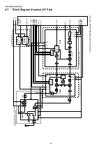
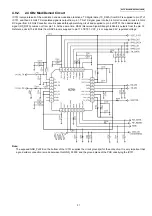
5.8 GHz Converter Circuit
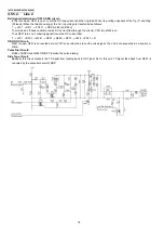
This block converts frequency of TX signal and RX signal.
IC801 includes TX-MIXER, RX-MIXER, PLL and VCO modules internally.
The VCO module is tuned by PLL synthesizer module, and generates 3.4 GHz Local signal. Reference clock (13.824 MHz) from
DSP block is supplied to pin 7 of IC701.
2.4 GHz TX signal from 2.4 GHz Mod/Demod circuit is supplied to pin 17 of IC801, and internal TX-MIXER multiplies it by 3.4 GHz
Local signal from internal VCO module, and up-converts into 5.8 GHz TX signal. This 5.8 GHz TX signal is output from pin 2, and
goes into the 5.8 GHz PA circuit.
5.8 GHz RX signal from 5.8 GHz LNA circuit supplied to pin 5 of IC801, and internal RX-MIXER multiplies it by 3.4 GHz Local signal
from internal VCO module, and down-converts into 2.4 GHz RX signal. This 2.4 GHz RX signal is output from pin 15, and goes into
the 2.4 GHz Mod/Demod circuits.
Note:
The exposed GND_PLATE on the bottom of the IC801 supplies the circuit ground(s) for the entire chip. It is very important that
a good solder connection is made between this GND_PLATE and the ground plane of the PCB underlying the IC801.
Содержание KX-TG6700BXB
Страница 2: ...2 KX TG6700BXB KX TGA670BXB ...
Страница 6: ...6 KX TG6700BXB KX TGA670BXB 3 Specifications ...
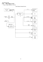
Страница 26: ...26 KX TG6700BXB KX TGA670BXB 4 8 2 Power Supply Circuit Voltage is supplied separately to each block ...
Страница 35: ...35 KX TG6700BXB KX TGA670BXB 4 11 Signal Route Each signal route is as follows ...
Страница 36: ...36 KX TG6700BXB KX TGA670BXB RF part signal route ...
Страница 37: ...37 KX TG6700BXB KX TGA670BXB 5 Location of Controls and Components 5 1 Controls 5 1 1 Base Unit ...
Страница 40: ...40 KX TG6700BXB KX TGA670BXB 6 1 2 Connecting the Telephone Line Cord ...
Страница 41: ...41 KX TG6700BXB KX TGA670BXB 6 1 2 1 If you subscribe to a DSL service ...
Страница 43: ...43 KX TG6700BXB KX TGA670BXB 6 4 1 Battery Level 6 4 2 Panasonic Battery Performance ...
Страница 44: ...44 KX TG6700BXB KX TGA670BXB 7 Operation Instructions 7 1 Symbols Used in These Operating Instructions ...
Страница 46: ...46 KX TG6700BXB KX TGA670BXB ...
Страница 47: ...47 KX TG6700BXB KX TGA670BXB 7 2 2 Programming Using the Direct Commands ...
Страница 48: ...48 KX TG6700BXB KX TGA670BXB ...
Страница 49: ...49 KX TG6700BXB KX TGA670BXB 7 3 Error Messages ...
Страница 50: ...50 KX TG6700BXB KX TGA670BXB 7 4 Troubleshooting ...
Страница 51: ...51 KX TG6700BXB KX TGA670BXB ...
Страница 52: ...52 KX TG6700BXB KX TGA670BXB ...
Страница 72: ...72 KX TG6700BXB KX TGA670BXB 10 1 9 5 RF DSP Interface Signal Wave Form Test Burst Mode ...
Страница 73: ...73 KX TG6700BXB KX TGA670BXB Test Burst Mode ...
Страница 80: ...80 KX TG6700BXB KX TGA670BXB 11 1 2 Handset ...
Страница 81: ...81 KX TG6700BXB KX TGA670BXB 11 1 3 Charger Unit ...
Страница 82: ...82 KX TG6700BXB KX TGA670BXB 11 2 Fix the LCD and the Receiver Guide to the Main P C Board Handset ...
Страница 93: ...93 KX TG6700BXB KX TGA670BXB Memo ...
Страница 97: ...97 KX TG6700BXB KX TGA670BXB Memo ...
Страница 106: ...106 KX TG6700BXB KX TGA670BXB Memo ...
Страница 116: ...116 KX TG6700BXB KX TGA670BXB 15 3 Explanation of IC Terminals RF Part 15 3 1 IC701 ...
Страница 117: ...117 KX TG6700BXB KX TGA670BXB 15 3 2 IC801 Backside Terminal GND ...
Страница 118: ...118 KX TG6700BXB KX TGA670BXB 15 3 3 IC851 Backside Terminal GND ...
Страница 119: ...119 KX TG6700BXB KX TGA670BXB 15 4 Terminal Guide of the ICs Transistors and Diodes 15 4 1 Base Unit 15 4 2 Handset ...
Страница 120: ...120 KX TG6700BXB KX TGA670BXB 16 Exploded View and Replacement Parts List 16 1 Cabinet and Electrical Parts Base Unit ...
Страница 122: ...122 KX TG6700BXB KX TGA670BXB 16 3 Cabinet and Electrical Parts Charger Unit ...
Страница 123: ...123 KX TG6700BXB KX TGA670BXB 16 4 Accessories and Packing Materials 16 4 1 KX TG6700BXB ...
Страница 124: ...124 KX TG6700BXB KX TGA670BXB 16 4 2 KX TGA670BXB ...

