background image

73

KX-TG6700B/KX-TG6702B/KX-TGA670B

10.1.9.4. TEST RANGE Check

Circuit block which range is defective can be found by the following check.

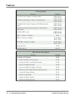
CHART1: Setting of TX Power and RX Sensitivity in Range Confirmation TX TEST, RX TEST

Note:

(*1) 

Adjustment and Test Mode Flow Chart

 (P.55)

Item

BU (Base Unit) Check

HS (HandSet) Check

Range Confirmation TX TEST
(TX Power check)

HS, BU Mode:
 [Test Link Mode] (*1)

1. Register Regular HS to BU (to be checked).
2. Set BU to “Test Link mode”.
3. Set Regular HS to “Test Link mode”.

*Set TX Power and RX Sensitivity of the BU and the
Regular HS by CHART1.

* At distance of about 20 m between HS and BU,
Link OK = TX Power of the BU is OK.
No Link = TX Power of the BU is NG.

1. Register HS (to be checked) to Regular BU.
2. Set Regular BU to “Test Link mode”.
3. Set HS to “Test Link mode”.

*Set TX Power and RX Sensitivity of the HS and the
Regular BU by CHART1.

* At distance of about 20 m between HS and BU,
Link OK = TX Power of the HS is OK.
No Link = TX Power of the HS is NG.

Range Confirmation RX TEST
(RX sensitivity check)

HS, BU Mode:
[Test Link Mode] (*1)

1. Register Regular HS to BU (to be checked).
2. Set BU to “Test Link mode”.
3. Set Regular HS to “Test Link mode”.

*Set TX Power and RX Sensitivity of the BU and Regular
HS by CHART1.

* At distance of about 20 m between HS and BU,
Link OK= RX Sensitivity of the BU is OK.
No Link = RX Sensitivity of the BU is NG.

1. Register HS (to be checked) to Regular BU.
2. Set Regular BU to “Test Link mode”.
3. Set HS to “Test Link mode”.

* Set TX Power and RX Sensitivity of Checking_HS and
Regular_BU by CHART1.

* At distance of about 20 m between HS and BU,
Link OK= RX Sensitivity of the HS is OK.
No Link = RX Sensitivity of the HS is NG

BU (to be checked)

Regular_HS

TX Power

RX Sens.

TX Power

RX Sens.

BU (Base Unit) TX Power Check

High

High

High

Low

BU (Base Unit) RX Sensitivity Check

High

High

Low

High

HS (to be checked)

Regular_BU

TX Power

RX Sens.

TX Power

RX Sens.

HS (Handset) TX Power Check

High

High

High

Low

HS (Handset) RX Sensitivity Check

High

High

Low

High

Содержание KX-TG6700B - Cordless Phone - Operation

Страница 1: ...opying and distribu tion is a violation of law ORDER NO KM40604038CE F12 Telephone Equipment KX TG6700B KX TG6702B KX TGA670B 5 8 GHz Expandable Digital Cordless Answering System 5 8 GHz Expandable Digital Cordless Answering System with Two Handsets Black Version for U S A ...

Страница 2: ...2 KX TG6700B KX TG6702B KX TGA670B ...

Страница 3: ...w to Replace the LLP Leadless Leadframe Package IC 79 11 Disassembly and Assembly Instructions 81 11 1 Disassembly Instructions 81 11 2 Fix the LCD and the Receiver Guide to the Main P C Board Handset 84 12 Measurements and Adjustments 85 12 1 Things to Do after Replacing IC 85 12 2 Base Unit Reference Drawing 86 12 3 Handset Reference Drawing 87 12 4 Frequency Table 88 13 Schematic Diagram 90 13 ...

Страница 4: ...o standard solder or solder that con tains lead We will use PbF solder when discussing the lead free solder used in our manufacturing process which is made from Tin Sn Silver Ag and Copper Cu This model and others like it manufactured using lead free solder will have PbF stamped on the PCB For service and repair work we suggest using the same type of solder Caution PbF solder has a melting point t...

Страница 5: ...ecific instructions for the melting points of their products and any precautions for using their product with other materi als The following lead free PbF solder wire sizes are recommended for service of this product 0 3 mm 0 6 mm and 1 0 mm 2 2 2 How to Recognize that Pb Free Solder is Used Example Handset P C B Component View Note The location of the PbF mark is subject to change without notice ...

Страница 6: ...6 KX TG6700B KX TG6702B KX TGA670B 3 Specifications ...

Страница 7: ...quencies of the Base Unit and Handset are shared in the same frequency The construction of RX TX frequency data is shown below It consists of 4 slots from the Base Unit to the Handset and 4 slots from the Handset to the Base Unit total 8 slots in 10 ms By this slot system simultaneous air link and communication between 4 Handsets and the Base Unit can be realized One communication between Handset ...

Страница 8: ... possible to perform four duplex communications simultaneously Up to eight Handsets can be registered In 1 slot 1 25 ms the 10 ms of voice data is transmitted Each slot makes every frame frequency hop 100 hops sec Although each slot UpLink3 and UpLink4 uses different frequency UpLink3 and DownLink3 use the same frequency 2 Handsets Link Traffic Bearer A link is established between Base Unit and Ha...

Страница 9: ...TA then enter to DSP IC201 The DSP performs TDD TDMA and ADPCM decoding to convert the RXDATA into the voice signal then it is output to the speaker Transmission The voice signal entering from the Handset microphone is led to DSP IC201 The DSP encodes ADPCM and TDD TDMA with FHSS to TXMOD The TXMOD signal is enter to IC701 of RF PART and modulated to 2 4 GHz The 2 4 GHz signal is up converted to 5...

Страница 10: ...10 KX TG6700B KX TG6702B KX TGA670B 4 2 Explanation of Link Data Communication 4 2 1 Calling 4 2 2 To Terminate Communication 4 2 3 Ringing ...

Страница 11: ...VCCPA V_RF VCC ANSWER_LED SP PHONE_LED LINE2_LED IC601 FLASH MEMORY LCD KEYS IC300 Q300 Q171 RSSI SHCTRL RADIO_EN TX_EN RX_EN LO_EN SYN_DATA SYN_CLK OSC_IN SYN_LE2 TXDATA V_RF VPA SI SO CS INUSE_LED COM1 COM2 SEG3 12 BCLK LINE1_LED MESSAGE_LED KEY1 6 KEYA F RXDATA MIP DCIN0 SYN_LE1 SYN_OUT RX_GAIN RF_RESET 3 3V REGULATOR with RESET CLK RST ANT0 ANT1 PA_CONT AC_DOWN Q340 AC DOWN RLY Photo Coupler I...

Страница 12: ...ace VCC 2 4GHz Mod Demod Circuit 2 4GHz 2 4GHz FL811 FL891 FL881 IC851 5 8GHz Power Amp 5 8GHz LNA and Antenna Switch Circuit V_PA V_RF RADIO_EN SYN_LE2 SYN_CLK SYN_DATA SYN_LE1 OSC_IN TX_EN SYN_OUT TX_DATA RX_DATA RSSI SHCTRL RF_RESET RX_EN RX_GAIN DSP PLL Serial Interface 5 8GHz Converter Circuit IC801 3 4GHz 5 8GHz PA_CONT VCC TXEN REFIN ANT0 ANT1 RXEN RXGAIN 5 8GHz FL821 KX TG6700 6702 BLOCK D...

Страница 13: ...m in software The DTMF detection is performed during Record Play back and Line Monitoring modes of operation When the DTMF data from the Handset is received the DTMF signal is output Synthesized Voice Pre recorded message The DSP implements synthesized Voice utilizing the built in speech detector and a Flash Memory which stored the vocabulary Caller ID and Call Waiting CID demodulation The DSP imp...

Страница 14: ...G6702B KX TGA670B 4 5 3 Power Supply Circuit Function The power supply voltage from AC adaptor is converted to the desired voltage of each block Circuit Operation Q300 and IC300 4 5 V DCDC Converter IC331 3 3 V Regulator ...

Страница 15: ...tor is supplied to the charge circuits Main charge 130 220 mA at the Battery of maximum 7 hours is started soon after the Handset is placed on the Base Unit Then it changes to Trickle charge to prevent from overcharging Q361 and Q362 detect the ON HOOK state Handset is placed on Base Unit ...

Страница 16: ...ncorporates an AC adaptor Circuit Operation When the AC Adaptor is inserted into the unit then the voltage is shifted by IC331 and power is supplied to the DSP The set starts to operate when VCC goes up to 3 0 V or more in the circuit voltage diagram Note 1 The initializing time of the DSP chip is 28 ms under normal conditions ...

Страница 17: ...101 R111 PC111 DSP pin 72 BELL To provide an off hook condition active DC current flow through the circuit CPU turns Q145 on Thus Q141 and Q142 turn on Following signal flow is the DC current flow T L101 D101 Q141 Q161 R163 Q142 D101 L102 P101 R ON HOOK Circuit Q141 is open Q141 is connected as to cut the DC loop current and to cut the voice signal The unit is consequently in on hook condition Pul...

Страница 18: ...e DC current flow through the circuit CPU turns Q246 on Thus Q241 turns on Following signal flow is the DC current flow T L201 D201 Q241 Q261 R263 D201 L202 P201 R ON HOOK Circuit Q241 is open Q241 is connected as to cut DC loop current and to cut the voice signal The unit is consequently in on hook con dition Pulse Dial Circuit Pin86 of DSP turns Q246 ON OFF to make the pulse dialing Side Tone Ci...

Страница 19: ...plifier with high value resisters is used in order to isolate both lines This circuit gain is controlled by the signal inverse RLY When the base unit is in off hook condition the control signal logic is zero This circuit transforms the voltage of the line and DSP monitors the result of the transformation When the DSP detects the voltage drop 0 2 V or more by parallel connected telephone off hook t...

Страница 20: ...20 KX TG6700B KX TG6702B KX TGA670B Line 2 You can enable or disable the Auto Disconnect function See Check Record P 66 ...

Страница 21: ...cally Circuit Operation The circuit is same as Auto Disconnect circuit But this circuit is controlled by inverse RLY signal In on hook state the input signal logic is high then the transistors Line 1 Q156 and Q136 Line 2 Q256 and Q236 turn on As a result the circuit gain is different from off hook state If the input signal to DSP is 1 65 V or higher DSP will judge there is no use of the telephones...

Страница 22: ...he data for the caller ID from the telephone exchange is sent during the interval between the first and second rings of the bell signal The data from the telephone exchange is a modem signal which is modulated in an FSK Frequency Shift Keying format Data 1 is a 1200 Hz sine wave and data a 2200 Hz sine wave There are two types of the message format which can be received i e the single message form...

Страница 23: ...cide whether to take the new call Function The telephone exchange transmits or receives CAS and ACK signals through each voice RX TX route Then FSK data and MARK data pass the following route Telephone Line 1 CN101 T R C121 C122 R121 R122 IC501 122 123 If the unit deems that a telephone connected in parallel is in use ACK is not returned even if CAS is received and the information for the second a...

Страница 24: ... DSP IBAT1 IBAT2 CHG_CTL CHG_DET RADIO_EN CON_EN SYN_LE2 SYN_OUT SYN_DATA SYN_CLK SYN_LE1 RX_GAIN RX_EN TX_EN SHCTRL RF_RESET RSSI WP CLK DATA LCD_LIGHT KEY_LIGHT KEYSTOROBE_A F KEYIN_1 5 R376 R379 Q362 Q363 CHARGE CONTROL CHARGE CURRENT POWER DOWN MIC SP Headset Jack CN331 Q331 LED261 HEADSET DETECT Monitor SP LCD KEYS RF part ANT X201 13 824MHz EEPROM OSC_IN PA_CONT TX_DATA RX_DATA Q262 IC373 Q3...

Страница 25: ...erface VCC 2 4GHz Mod Demod Circuit 2 4GHz 2 4GHz FL811 IC851 5 8GHz Power Amp 5 8GHz LNA and Antenna Switch Circuit V_PA V_RF RADIO_EN CON_EN SYN_LE2 SYN_CLK SYN_DATA SYN_LE1 OSC_IN TX_EN SYN_OUT TX_DATA RX_DATA RSSI SHCTRL RF_RESET RX_EN RX_GAIN DSP PLL Serial Interface 5 8GHz Converter Circuit IC801 3 4GHz 5 8GHz PA_CONT VCC TXEN REFIN RXEN RXGAIN 5 8GHz FL821 KX TGA670 BLOCK DIAGRAM Handset_RF...

Страница 26: ...on Battery Low Power down detect circuit Ringer Generation Interface circuit RF part Speaker Mic LED Key scan LCD Headset Initialize Note 1 The initializing time of the DSP chip is 20 ms under normal conditions 4 8 1 2 RF part Mainly voice signal is modulated to RF or it goes the other way 4 8 1 3 EEPROM IC241 All setting data is stored ex ID code user setting Phonebook Caller ID data ...

Страница 27: ...27 KX TG6700B KX TG6702B KX TGA670B 4 8 2 Power Supply Circuit Voltage is supplied separately to each block ...

Страница 28: ... R366 and D361 The voltage between CHARGE and CHARGE flows R231 Q231 pin 41 of IC201 where the charge is detected Then IC201 calculates the battery consumption amount from the previous charge and it controls Q361 Q362 Q363 by pin 79 of IC201 until charging is complete When charging is complete the control pattern is switched to Trickle charging form from Operational charging form 4 8 4 Ringer and ...

Страница 29: ...adset is input to DSP 94 Also the power for the microphone is supplied from DSP 78 and the power is turned OFF on standby 4 8 6 Reception Signal The voice signal from the Base Unit is output to DSP 97 This signal is led to the headset jack CN331 The signal through the headset jack and the other signal output from DSP 96 drives the speaker When the headset is inserted to the jack the voice signal i...

Страница 30: ...t Operation RF Part General Description RF part includes Transmitter and Receiver functions Digital signals Mainly voice data that come from DSP are modulated and are transmitted On the other hand received signals are demodulated and go out to DSP ...

Страница 31: ...bout 4 0 V at Base Unit or 3 1 V at Handset is supplied to the Power amplifier in 5 8 GHz PA circuit IC841 is 3 0 V Base Unit or 2 8 V Handset Regulators and IC761 is a 2 5 V Regulator They output Vcc_5 8 GHz and Vcc_2 4 GHz respectively by order of RADIO_EN signal or CON_EN signal V_RF is approximately 4 0 V Base Unit or 3 1 V Handset ...

Страница 32: ...uit is passed through matching circuit and supplied to pin 4 of IC701 then demodulated signal RX_DATA comes out from pin 16 At the same time RSSI Received Signal Strength Indicator outputs from the pin 14 Reference clock 13 824 MHz from DSP block is supplied to pin 11 of IC701 VCC_2 4 G supplies 2 5 V regulated voltage Note The exposed GND_PLATE on the bottom of the IC701 supplies the circuit grou...

Страница 33: ...l signal from internal VCO module and up converts into 5 8 GHz TX signal This 5 8 GHz TX signal is output from pin 2 and goes into the 5 8 GHz PA circuit 5 8 GHz RX signal from 5 8 GHz LNA circuit supplied to pin 5 of IC801 and internal RX MIXER multiplies it by 3 4 GHz Local signal from internal VCO module and down converts into 2 4 GHz RX signal This 2 4 GHz RX signal is output from pin 15 and g...

Страница 34: ...a terminal Note The exposed GND_PLATE on the bottom of the IC851 supplies the circuit ground s for the entire chip It is very important that a good solder connection is made between this GND_PLATE and the ground plane of the PCB underlying the IC851 Base Unit IC851 includes Switches for High frequency signals and controlled by ANT0 signal and ANT1 signal from DSP DSP is checking RSSI Received Sign...

Страница 35: ...pplied to the charge circuits Main charge 130 220 mA at the Battery of maximum 7 hours is started soon after the Handset is placed on the Charger Unit Then it changes to Trickle charge to prevent from overcharging The route for this is as follows DC pin of CN1 R1 R3 CHARGE pad Handset CHARGE pad DC pin of CN1 ...

Страница 36: ...36 KX TG6700B KX TG6702B KX TGA670B 4 11 Signal Route Each signal route is as follows ...

Страница 37: ...37 KX TG6700B KX TG6702B KX TGA670B RF part signal route ...

Страница 38: ...38 KX TG6700B KX TG6702B KX TGA670B 5 Location of Controls and Components 5 1 Controls 5 1 1 Base Unit ...

Страница 39: ...39 KX TG6700B KX TG6702B KX TGA670B 5 1 2 Handset 5 2 Displays 5 2 1 Base Unit Display Items 5 2 2 Handset Display Items ...

Страница 40: ...40 KX TG6700B KX TG6702B KX TGA670B 6 Installation Instructions 6 1 Setting Up the Base Unit 6 1 1 Connecting the AC Adaptor ...

Страница 41: ...41 KX TG6700B KX TG6702B KX TGA670B 6 1 2 Connecting the Telephone Line Cord ...

Страница 42: ...42 KX TG6700B KX TG6702B KX TGA670B 6 1 2 1 If you subscribe to a DSL service ...

Страница 43: ...43 KX TG6700B KX TG6702B KX TGA670B 6 2 Setting Up the Handset 6 2 1 Connecting the Charger KX TG6702 only 6 3 Battery Installation Replacement ...

Страница 44: ...ngth may not be indicated correctly if the battery is disconnected and connected again even after it is fully charged In that case by recharging the battery as mentioned above you will get a correct indication of the battery strength 6 4 1 Battery Level 6 4 2 Panasonic Battery Performance ...

Страница 45: ...45 KX TG6700B KX TG6702B KX TGA670B 7 Operation Instructions 7 1 Symbols Used in These Operating Instructions ...

Страница 46: ...46 KX TG6700B KX TG6702B KX TGA670B 7 2 Programmable Settings 7 2 1 Programming by Scrolling through the Display Menus ...

Страница 47: ...47 KX TG6700B KX TG6702B KX TGA670B ...

Страница 48: ...48 KX TG6700B KX TG6702B KX TGA670B 7 2 2 Programming Using the Direct Commands ...

Страница 49: ...49 KX TG6700B KX TG6702B KX TGA670B ...

Страница 50: ...50 KX TG6700B KX TG6702B KX TGA670B 7 3 Error Messages ...

Страница 51: ...51 KX TG6700B KX TG6702B KX TGA670B 7 4 Troubleshooting If the display shows error messages see Error Messages P 50 for the Cause Solution ...

Страница 52: ...52 KX TG6700B KX TG6702B KX TGA670B ...

Страница 53: ...53 KX TG6700B KX TG6702B KX TGA670B ...

Страница 54: ...54 KX TG6700B KX TG6702B KX TGA670B ...

Страница 55: ...0B 8 Test Mode 8 1 Adjustment and Test Mode Flow Chart 8 1 1 Test Burst Mode for Base Unit Note 1 LCD displays the Channel number 2 Refer to Check Table for RF part P 72 and RX CW Test Mode for Handset P 60 for proper Handset settings ...

Страница 56: ...G6700B KX TG6702B KX TGA670B 8 1 2 RX CW Test Mode for Base Unit Note 1 LCD displays the Channel number 2 Refer to Check Table for RF part P 72 and Test Burst Mode for Handset P 59 for proper Handset settings ...

Страница 57: ... displays the number of selected power 3 Refer to Test Link Mode for Handset P 61 If can not proceed to the next step refer to Registering a Handset P 70 4 Refer to Check Table for RF part P 72 and Test Burst Mode for Handset P 59 for proper Handset settings 5 Display may vary according to the receiving sensitivity ...

Страница 58: ...58 KX TG6700B KX TG6702B KX TGA670B 8 1 4 Adjustment Mode for Base Unit Cross Reference Check and Adjust X501 Base Unit Frequency P 85 Note 1 This is an adjustment value hex ...

Страница 59: ...02B KX TGA670B 8 1 5 Test Burst Mode for Handset Note 1 LCD displays the Channel number exception default CH00 1ch 2 Refer to Check Table for RF part P 72 and RX CW Test Mode for Base Unit P 56 for proper Base Unit settings ...

Страница 60: ...02B KX TGA670B 8 1 6 RX CW Test Mode for Handset Note 1 LCD displays the Channel number exception default CH00 1ch 2 Refer to Check Table for RF part P 72 and Test Burst Mode for Base Unit P 55 for proper Base Unit settings ...

Страница 61: ...Note 1 LCD displays the Channel number exception default CH00 1ch 2 If can not proceed to the next step refer to Registering a Handset P 70 3 for factory use only 4 Refer to Check Table for RF part P 72 and Test Link Mode for Base Unit P 57 for proper Base Unit settings ...

Страница 62: ...G6702B KX TGA670B 8 1 8 Adjustment Mode for Handset Cross Reference 1 Adjust Battery Low Detector Voltage Handset P 85 Note 2 These are the default values 3 These values may not be fixed depending on the battery strength ...

Страница 63: ...on Erase recorded Voice messages stored Phone numbers Caller list and etc This operation should not be performed for a usual repair 9 1 1 Base Unit Note 1 Telephone line must be connected 9 1 2 Handset Note 1 Be sure to short the battery terminals of the Handset with a lead wire etc for 2 seconds for discharge after removing the battery ...

Страница 64: ... Sp phone Reception P 67 Check Battery Charge P 68 Check Link P 69 Check the RF part P 70 Check Handset Transmission P 76 Check Handset Reception P 76 Check Caller ID P 76 Note 1 When a user claims that the unit disconnects a call right after the greeting message and no incoming messages can be recorded this symptom can not be reappeared with TEL simulator in the service center So in that case try...

Страница 65: ... Table Note Flash Memory is IC601 DSP is IC501 Display Symptom Remedy E1 The initialization was tried but it could not be done 1 Check the peripheral circuit of Flash Memory visually 2 Confirm that the voltage is added to the power supply pin If no voltage is detected replace the Flash Memory because it might be defect 3 Solder the Flash Memory again E3 E9 When the adjustment data was checked an e...

Страница 66: ...arallel connected telephone is OFF HOOK the line isn t disconnected D How to change the VOX level It makes easier to detect a small voice caller by raising the sensitivity of VOX level Therefore the recording of TAM is not turned off during a detection Cross Reference Signal Route P 36 Telephone Line Interface P 17 Auto Disconnect Circuit P 19 Parallel Connection Detect Circuit P 21 Note Flash Mem...

Страница 67: ...lash Memory is IC601 DSP is IC501 10 1 5 Check Sp phone Transmission Cross Reference Signal Route P 36 Telephone Line Interface P 17 Note Flash Memory is IC601 DSP is IC501 10 1 6 Check Sp phone Reception Cross Reference Telephone Line Interface P 17 Signal Route P 36 Note Flash Memory is IC601 DSP is IC501 ...

Страница 68: ...68 KX TG6700B KX TG6702B KX TGA670B 10 1 7 Check Battery Charge Note Flash Memory is IC601 DSP is IC501 1 Refer to Specifications P 6 for part number and supply voltage of AC adaptor ...

Страница 69: ...69 KX TG6700B KX TG6702B KX TGA670B 10 1 8 Check Link Note Flash Memory is IC601 DSP is IC501 1 Refer to Finding out the Defective part P 70 Cross Reference Check the RF part P 70 ...

Страница 70: ...eck the RF part 10 1 9 1 Finding out the Defective part After All the Checkings or Repairing 1 Re register the checked Handset to the checked Base Unit and Regular HS to Regular BU Note 1 HS Handset 2 BU Base Unit 10 1 9 1 1 Registering a Handset ...

Страница 71: ...KX TG6700B KX TG6702B KX TGA670B 10 1 9 1 2 Deregistering a Handset 10 1 9 2 RF Check Flowchart Each item 1 6 of RF Check Flowchart corresponds to Check Table for RF part P 72 Please refer to the each item ...

Страница 72: ... RX CW Mode 4 HS BU to be checked Mode Test Burst Mode 1 1 Place the Regular HS about 15 cm away from the BU 2 Confirm that RSSI of the Regular HS is approximately 2 V by Oscilloscope 5 1 Place the HS about 15 cm away from the Regular BU 2 Confirm that RSSI of the Regular BU is approximately 2 V by Oscilloscope 6 5 RX Sensitivity confirmation Regular HS BU Mode Test Burst Mode 1 HS BU to be checke...

Страница 73: ...etween HS and BU Link OK TX Power of the HS is OK No Link TX Power of the HS is NG Range Confirmation RX TEST RX sensitivity check HS BU Mode Test Link Mode 1 1 Register Regular HS to BU to be checked 2 Set BU to Test Link mode 3 Set Regular HS to Test Link mode Set TX Power and RX Sensitivity of the BU and Regular HS by CHART1 At distance of about 20 m between HS and BU Link OK RX Sensitivity of ...

Страница 74: ...74 KX TG6700B KX TG6702B KX TGA670B 10 1 9 5 RF DSP Interface Signal Wave Form Test Burst Mode ...

Страница 75: ...75 KX TG6700B KX TG6702B KX TGA670B Test Burst Mode ...

Страница 76: ...RF part Refer to Check the RF part P 70 10 1 12 Check Caller ID Cross Reference Telephone Line Interface P 17 Calling Line Identification Caller ID Call Waiting Caller ID P 22 Note Make sure the format of the Caller ID or Call Waiting Caller ID service of the Telephone company that the customer sub scribed to Also we recommend to confirm that the customer is really a subscriber of the service ...

Страница 77: ...age the PCB foil Flux Recommended Flux Specific Gravity 0 82 Type RMA lower residue non cleaning type Note See About Lead Free Solder Pbf Pb free P 4 10 2 2 How to Remove the IC 1 Put plenty of solder on the IC pins so that the pins can be completely covered Note If the IC pins are not soldered enough you may give pressure to the P C board when cutting the pins with a cutter 2 Make a few cuts into...

Страница 78: ... of the IC setting with the corresponding soldering foil 2 Apply flux to all pins of the FLAT PACKAGE IC 3 Solder the pins sliding the soldering iron in the direction of the arrow 10 2 4 How to Remove a Solder Bridge 1 Lightly resolder the bridged portion 2 Remove the remaining solder along the pins using a soldering iron as shown in the figure below ...

Страница 79: ... IC efficiently choose the right sized nozzle of the hot air desoldering tool that matches the IC package Be careful about the temperature of the hot air desoldering tool not to damage the PCB and or IC 10 3 3 How to Remove the IC 1 Heat the IC with a hot air desoldering tool through the P C Board 2 Pick up the IC with tweezers etc when the solder is melted completely Note Be careful not to touch ...

Страница 80: ...he IC the positioning should be done very carefully 3 Heat the IC with a hot air desoldering tool through the P C Board until the solder on IC bottom is melted Note Be sure to place it precisely controlling the air volume of the hot air desoldering tool 4 After soldering confirm there are no short and open circuits with visual inspection 10 3 5 How to Remove a Solder Bridge When a Solder Bridge is...

Страница 81: ...81 KX TG6700B KX TG6702B KX TGA670B 11 Disassembly and Assembly Instructions 11 1 Disassembly Instructions 11 1 1 Base Unit ...

Страница 82: ...82 KX TG6700B KX TG6702B KX TGA670B 11 1 2 Handset ...

Страница 83: ...83 KX TG6700B KX TG6702B KX TGA670B 11 1 3 Charger Unit ...

Страница 84: ...84 KX TG6700B KX TG6702B KX TGA670B 11 2 Fix the LCD and the Receiver Guide to the Main P C Board Handset ...

Страница 85: ...adjust to Adjustment tolelance 30 Hz by pressing or key Adjustment Tolerance 13 824 MHz 30 Hz 5 Press TALK key to write the new frequency factor in EEPROM 6 Turn the power off Then this value is available Cross Reference Adjustment Mode for Handset P 62 12 1 2 Adjust Battery Low Detector Voltage Handset After Handset s DSP IC201 or EEPROM IC241 replacement Re writing Battery Low voltage to EEPROM ...

Страница 86: ...1 FCLK Q361 Q362 RA501 RA500 Q151 Q171 INT1 Q161 BCLK2 RSSI FCS FSO FSI UVCC Q145 RST Q136 Q141 D101 PC111 Q340 Q300 CN301 CN101 CN201 ANT0 Q142 Q156 Q271 DA214 DA213 Q236 Q245 Q261 PC211 PC141 PC241 PC242 Q241 D201 Q246 Q256 T281 T261 L472 L361 L371 D473 D472 D361 D362 RED CHG SP WHITE MIC MIC C383 C341 X501 C300 D300 D301 C306 SA101 SA202 SA201 SA104 ANT1 L300 L101 L102 L202 L201 P101 P201 R373 ...

Страница 87: ...C305 C306 C336 C333 C313 D312 D313 R378 R368 R241 R242 C242 C244 C354 C315 C243 C209 C241 R205 R207 R261 Q261 Q262 R206 C206 R209 C377 C316 R314 C379 R379 C303 C314 C226 R226 R312 R201 R225 R232 C202 C212 C215 C225 R227 C201 C211 C219 D326 D327 L326 SP L327 R246 R329 C246 R247 R263 R375 R374 R234 C371 C263 C264 C362 C361 C373 C262 C261 R331 R264 R324 R262 L332 L373 D373 Q373 L334 C322 C335 C321 C3...

Страница 88: ...87 12 5769 510992 44 5798 050836 76 5826 590680 13 5770 404840 45 5798 944684 77 5827 484527 14 5771 294732 46 5799 834576 78 5828 374420 15 5772 188580 47 5800 728424 79 5829 268268 16 5773 078473 48 5801 618316 80 5830 158160 17 5773 972320 49 5802 512164 81 5831 052008 18 5774 862213 50 5803 402057 82 5831 941900 19 5775 756060 51 5804 295904 83 5832 835748 20 5776 645953 52 5805 185797 84 5833...

Страница 89: ...512974 44 5798 052818 76 5826 592662 13 5770 402867 45 5798 942710 77 5827 482554 14 5771 296714 46 5799 836558 78 5828 376402 15 5772 186607 47 5800 726451 79 5829 266294 16 5773 080455 48 5801 620298 80 5830 160142 17 5773 970347 49 5802 510191 81 5831 050035 18 5774 864195 50 5803 404039 82 5831 943882 19 5775 754087 51 5804 293931 83 5832 833775 20 5776 647935 52 5805 187779 84 5833 727623 21 ...

Страница 90: ...set_Main Notes 1 DC voltage measurements are taken with an oscilloscope or a tester with a ground 2 The schematic diagrams may be modified at any time with the development of new technology 13 1 2 1 Microphone Input Level Handset Handset Mode Adjust the signal level to 40 dBm with 600 ohm load Then input the signal to MICP and MICN of the handset through the 47 µF capacitors Headset Mode Adjust th...

Страница 91: ... terminal volume max Handset SP RX 35 dBm 4 dBm 8 ohm terminal volume max Headset RX 25 dBm 20 5 dBm 150 ohm terminal volume max Line Input Level Output Level Remarks Base SP TX 47 dBm 15 5 dBm Refer to Microphone Input Level Base Unit P 90 Handset TX 40 dBm 15 5 dBm Refer to Microphone Input Level Handset P 90 Headset TX 44 dBm 15 5 dBm Refer to Microphone Input Level Handset P 90 ...

Страница 92: ... 103 104 105 106 107 108 109 110 111 112 113 114 115 116 117 118 119 120 121 122 123 124 125 126 127 128 1 2 3 4 5 6 7 8 9 10 11 12 13 14 15 16 17 18 19 20 21 22 23 24 25 26 27 28 29 30 31 32 33 34 35 36 37 38 39 40 41 42 43 44 45 46 47 48 49 50 51 52 53 54 55 56 57 58 59 60 61 62 63 64 65 66 67 68 69 70 71 72 73 74 75 76 77 78 79 80 81 82 83 84 85 86 87 88 89 90 91 92 93 94 95 96 97 98 99 100 101...

Страница 93: ...T L1R 10u 16V C166 33u L101 33u L102 Q151 NC 1 2 3 Q362 1 3 2 47k R362 NC R363 C165 K0 047 C163 K4700P 50V C162 J100P C167 K0 22 C331 K0 47 C308 K0 1 K680P 50V C122 K680P 50V C121 K0 047 C184 C185 K0 018 NC C171 NC C174 NC C175 NC C177 NC C173 NC C183 NC C182 D101 4 3 1 2 D362 1 2 100k R158 22p C152 1 AOUT 2 A IN 3 A IN 4 GND 5 B IN 6 B IN 7 BOUT 8 V 820k R136 68k R152 47k R111 27k R155 100n C136 ...

Страница 94: ...R235 820k R236 10k R237 2 7k R238 100k R241 10k R242 10k R243 3 3k R245 68k R252 47k R254 27k R255 10k R256 3 9k R257 100k R258 39k R262 47 R264 1 2k R265 560 R266 1k R267 0 R268 68 R271 150k R272 560 R275 100 R276 1k R278 2 7k R283 6 8k R285 68k R289 47k R290 68k R291 47k R292 47k R293 100k R294 680k R295 270k R296 10k R297 47k R298 NC R299 C261 10u 25V C267 K0 22 2 2M R213 2 2M R214 P201 22 33u ...

Страница 95: ...95 KX TG6700B KX TG6702B KX TGA670B Memo ...

Страница 96: ... PA_OUT 22 GND_ISO6 23 GND_ISO7 24 TRSW_IN 1 GND_ISO1 2 ANT1 3 GND_ISO2 J100P C833 18 R823 FL881 5 8GHz_LPF 2 1 4 3 B0 1P C871 K1 0 C857 NC R862 NC R812 3 3k R834 L871 3 3nH FL821 5 8GHz_BPF 1 2 3 4 C2P C873 K0 033 C809 L821 NC 5 8G_RF 4 GND_ISOL2 5 RX 6 VCC_LNA 7 REFIN 8 REFOUT 9 RXGAIN 10 CP_OUT 11 TV_IN 12 VARGND 13 PLL_BYP 14 VCC_PLL 15 2G4_OUT 16 GND_ISOL3 17 2G4_IN 18 VCC_TXRX 19 SYN_CLK 20 ...

Страница 97: ... C712 OSC_IN 330 R742 NC C841 D10P C747 VPA 2 4G_RF 1 TX 2 GND_ISO1 9 VCC_IF 3 GND_ISO2 4 RX 5 VCC_RF 6 VCC_IF2 7 TESTP 8 TESTN 10 XOUT 11 XIN 12 VCC_BIAS 13 REXT 14 RSSI 15 RSTN 16 RXDATA 17 TC_CTRL 18 VCC_DIG 19 VCC_PLL1A 20 VCC_PLL1B 21 TXEN 22 RXEN 23 VCC_PLL2B 24 VCC_PLL2A 25 RXGAIN 26 PA_RAMP 27 TXMOD 28 SYN_CLK 29 SYN_EN 30 SYN_DATA 31 SYN_OUT 32 VCC_PA 33 PADDLE_GND SYN_LE1 L724 NC C1 5P C...

Страница 98: ...F 1 2 MEMO 1 2 ERASE 1 2 L5DC01 2LINE LCD 1 2 3 4 5 6 7 8 9 10 11 12 ANS2 1 2 ANS1 1 2 SKIP 1 2 UP 1 2 DOWN 1 2 RPT 1 2 SP1SP2 L2 1 2 L1 1 2 INT 1 2 LED901 RED 1 2 LED902 GREEN 1 2 LED904 RED 1 2 LED905 RED 1 2 LED907 RED 1 2 LED909 RED 1 2 1 2 1 1 2 2 1 2 3 1 2 4 1 2 5 1 2 6 1 2 7 1 2 8 1 2 9 1 2 0 1 2 SHA 1 2 REDIAL 1 2 FLS 1 2 MUTE 1 2 SP 1 2 SP_LED KEYS_C KEYIN6 KEYIN5 LINE1_LED LINE2_LED INUS...

Страница 99: ...99 KX TG6700B KX TG6702B KX TGA670B Memo ...

Страница 100: ...CN271 8 SI CN271 1 NC CN271 3 NC CN271 12 CAP3 CN271 2 NC CN271 13 CAP1 CN271 14 CAP1 CN271 7 SCL CN271 17 V1 CN271 11 VOUT CN271 10 VSS CN271 21 V0 CN271 9 VDD CN271 22 NC CN271 6 AOP CN271 16 CAP2 82 R261 0 R264 4 RSSI 5 XIN 6 XOUT 7 VDD 8 VCCIN 9 GND 10 GND 11 GND 12 VCC 13 DCDCGND 14 KEY_BL 15 DCDCOUT 16 RSTN 17 FL_RST 18 FL_DO 19 FL_DI 20 FL_CS 21 NC 22 SYN_OUT 29 SHCTRL 30 GND 31 VCC 32 SYN_...

Страница 101: ...2k R226 270k R243 10 R208 K0 1 C226 K0 1 C225 K0 1 C306 NC R205 NC R206 NC R207 NC C307 PDN NC C243 NC C244 NC C209 1uF C303 C208 10uF 6 3V C304 NC NC C354 NC R367 K0 1 C231 VSS2 220k R374 NC R368 22k R231 Q231 1 3 2 K0 1 C374 Q362 1 3 2 2 0V_Reset 4 VSS 3 NC 1 OUT 2 VDD C373 330uF 16V CHG1 NC R230 CHG2 C361 330uF 16V 47k R363 NC C351 K1 0 C372 NC L351 NC R232 Q373 1 3 2 BATTP 47k R361 NC C352 BAT...

Страница 102: ...OUT 9 RXGAIN 10 CP_OUT 11 TV_IN 12 VARGND 13 PLL_BYP 14 VCC_PLL 15 2G4_OUT 16 GND_ISOL3 17 2G4_IN 18 VCC_TXRX 19 SYN_CLK 20 SYN_EN 21 SYN_DATA 22 RXEN 23 TXEN 24 VCC_PA1 1 VCC_PA2 2 TX 3 GND_ISOL1 5 8G_PA 4 GND_ISO3 5 ANT2 6 GND_ISO4 7 VDD_LNA1 8 GND_LNA1 9 VDD_LNA2 10 GND_LNA2 11 NC 12 LNA_OUT 13 LNA_GAIN 14 LNA_EN 15 ANTSEL_B 16 ANTSEL_A 17 PA_EN 18 PA_IN 19 VDD_PA 20 GND_ISO5 21 PA_OUT 22 GND_I...

Страница 103: ...1 SYN_CLK TX_DATA RX_EN TX_EN RX_DATA SYN_OUT SHCTRL RF_RESET OSC_IN RX_GAIN GND NC C769 NC C768 NC C765 NC C766 NC C846 NC C736 NC C845 J100P C837 K1uF 1608 C842 L711 18nH L724 NC L860 NC C723 2 7nH C701 4 7uF 2125 C843 K0 47 1608 C763 K0 47 1608 C762 NC 1608 L768 NC C0 5P C859 C0 5P C858 2 4G_RF 1 TX 2 GND_ISO1 9 VCC_IF 3 GND_ISO2 4 RX 5 VCC_RF 6 VCC_IF2 7 TESTP 8 TESTN 10 XOUT 11 XIN 12 VCC_BIA...

Страница 104: ...104 KX TG6700B KX TG6702B KX TGA670B 13 7 Schematic Diagram Charger Unit SCHEMATIC DIAGRAM Charger Unit NC No Components DCP DCM CM G CP CN1 2 1 R4 NC 56 R1 56 R2 56 R3 6 5 11V ...

Страница 105: ...SA202 SA201 SA104 C302 C301 ANT1 C303 C305 C323 L300 L101 L102 L202 L201 P101 P201 C322 C152 C138 C277 C272 C278 C274 C297 C296 C276 C275 C271 C292 C218 C238 C252 C235 C264 C214 C213 C211 C251 C289 C236 C266 C265 C263 C262 C260 C242 C202 C201 C261 C283 C281 C282 C284 C285 C217 C290 C267 C298 C135 C151 C136 C279 C280 C142 C162 C171 C175 C172 C178 C177 C174 C176 R472 R571 R175 R373 D142 D133 R372 R3...

Страница 106: ...4 1 2 Flow Solder Side View KX TG6700 6702 CIRCUIT BOARD Base Unit Flow Solder Side View A L2T L2R L1R L1T DCM2 DCM DCP2 DCP VCC GND BCLK DVCC JC JS JI JO JG R Y B G MIN MIP 6702 6700 PQUP11395Z PbF UTX2 SPN KIN4 KIN3 SPP CHARGE CHARGE URX2 ...

Страница 107: ...C745 C734 C733 C732 C731 C751 C768 C761 C766 C841 C846 C842 C844 C845 C874 C873 C809 C713 C711 L711 L724 C707 C762 C708 C714 C837 C804 C801 C811 C824 C851 C852 C853 C862 C863 C864 C861 C865 C807 C802 C821 C725 C806 C712 C715 C716 C723 C717 C722 C706 C803 C773 C833 C832 C838 C834 C872 C704 C781 C703 SHIELD C702 C741 C743 C742 C835 C705 FL891 C891 C881 C856 C857 R813 FL811 FL881 FL821 IC701 IC841 IC...

Страница 108: ...108 KX TG6700B KX TG6702B KX TGA670B Memo ...

Страница 109: ...PbF L5DC01 ANS1 ANS2 SELECT ERASE CHK REC STOP MEMO INT MSG VM 5761 5766 5771 5776 6700 3 2 12 6 5 9 8 0 1 1 32 1 CN901 4 7 MUTE FLS REDIAL AUTO L1 UP RPT HOLD SP1 SP2 A CONF DOWN LED905 LED907 LED904 LED909 LED902 LED901 SP PQUP11396Z KX TG6700 6702 CIRCUIT BOARD Base Unit_Operation Component View ...

Страница 110: ...702B KX TGA670B 14 3 2 Flow Solder Side View PbF PQUP11396Z ON THIS SIDE 1 A 12 DON T ATTACH LCD HOLDER KXTG5761 66 71 76 6700 KX TG6700 6702 CIRCUIT BOARD Base Unit_Operation Flow Solder Side View 5761 5766 5771 5776 6700 ...

Страница 111: ...26 D327 L326 SP L327 R246 R329 C246 R247 R263 R375 R374 R234 C371 C263 C264 C362 C361 C373 C262 C261 R331 R264 R324 R262 L332 L373 D373 Q373 L334 C322 C335 C321 C374 C372 C286 C271 C276 C281 C284 C283 C282 R286 C386 C382 C383 C275 C274 C273 C271 C272 C859 C858 C768 C769 C747 C752 C751 C763 C764 C765 C749 C750 C748 C735 C734 C733 C732 C731 C743 C702 C704 C781 C703 C741 C782 C836 C834 C835 C833 C832...

Страница 112: ...de View KX TGA670 CIRCUIT BOARD Handset_Main Flow Solder Side View PQUP11387Z LED255 LED256 LED257 CN271 22 1 TGA570R KX TGA570R LEFT OFF TALK BACK NEXT UP DOWN PAUSE RIGHT MENU SP 1 2 3 4 5 6 7 8 9 0 MIC MIC MIC HOLD FLASH LED252 LED254 LED261 LED251 LED253 A ...

Страница 113: ...3 C702 C704 C781 C703 C741 C782 C836 C834 C835 C833 C832 C803 C725 C705 C706 C722 C723 C717 C716 C804 C714 C708 C762 C766 C761 C841 C846 C842 C844 C843 C845 C874 C873 C811 C801 R824 R813 R812 R814 R873 R823 R822 R833 R701 R751 R752 R724 R747 R735 R864 R809 R742 R744 R861 R865 R863 R862 R832 R834 C824 C851 C852 C853 C863 C864 C821 L821 L871 L711 L768 L860 L724 L782 C802 C807 C865 C861 C862 C806 C71...

Страница 114: ...Unit 14 6 1 Component View 14 6 2 Flow Solder Side View CIRCUIT BOARD Charger Unit Component View CP DCP A R1 CM DCM R2 R4 RED WHITE R3 PQUP11398Z PQLV30043 KX TG57 67 PbF CIRCUIT BOARD Charger Unit Flow Solder Side View 1 2 CN1 PQUP11398Z PbF PQLV30043 KX TG57 67 A ...

Страница 115: ...ROM_DATA D O High Low 57 SEG4 EROM_CLK D O High Low 58 SEG3 EROM_WP D O High Low 59 SP_LED D I O Off On 60 GND GND GND 61 VCC VCC VCC 62 INT0 NC D O 63 FLASH_CLK High Middle Low 64 KEY_STB_F D O Active Not 65 KEY_STB_E D O Active Not 66 KEY_STB_D D O Active Not 67 KEY_STB_C D O Active Not 68 KEY_STB_B D O Active Not 69 KEY_STB_A D O Active Not 70 LINE_SZ D O On Off 71 NOT_RLY D O On Hook Off Hook ...

Страница 116: ... means the port is controlled by the firmware Data in the blank colums are omitted because of the Analog I O 120 L2_LIN1 A I 121 GNDA GND 122 CID IN0 A I 123 CID IN1 A I 124 VCCA VCC 125 NC A O 126 NC A O 127 LIN0 A I 128 L2_DCIN0 A I PIN Description I O High High_Z Low ...

Страница 117: ...On Charge 42 NC D O Low 43 NC D O Low 44 NC D O Low 45 NC D O Low 46 NC D O Low 47 NC D O Low 48 LCD_SCL D O High Low 49 LCD_SI D O High Low 50 GND GND GND 51 VCC VCC VCC 52 LCD_RESET D O Normal Reset 53 NC FLASH_CLK D O High 54 NC ANT_LED1 D O Low 55 NC ANT_LED2 D O Low 56 ANT_LED D O On Off 57 LCD_BL D O On Off 58 LCD_CS D O High Low 59 NC D O Low 60 LCD_A0 D O High Low 61 NC LED_CTRL D O Low 62...

Страница 118: ...118 KX TG6700B KX TG6702B KX TGA670B 15 3 Explanation of IC Terminals RF Part 15 3 1 IC701 ...

Страница 119: ...119 KX TG6700B KX TG6702B KX TGA670B 15 3 2 IC801 Backside Terminal GND ...

Страница 120: ...120 KX TG6700B KX TG6702B KX TGA670B 15 3 3 IC851 Backside Terminal GND ...

Страница 121: ...121 KX TG6700B KX TG6702B KX TGA670B 15 4 Terminal Guide of the ICs Transistors and Diodes 15 4 1 Base Unit 15 4 2 Handset ...

Страница 122: ...122 KX TG6700B KX TG6702B KX TGA670B 16 Exploded View and Replacement Parts List 16 1 Cabinet and Electrical Parts Base Unit ...

Страница 123: ...700B KX TG6702B KX TGA670B 16 2 Cabinet and Electrical Parts Handset Note 1 Stick the magnetic shield No 124 to the exact location described above 2 Attach the cushion No 128 to the exact location described above ...

Страница 124: ...124 KX TG6700B KX TG6702B KX TGA670B 16 3 Cabinet and Electrical Parts Charger Unit ...

Страница 125: ...125 KX TG6700B KX TG6702B KX TGA670B 16 4 Accessories and Packing Materials 16 4 1 KX TG6700B ...

Страница 126: ...126 KX TG6700B KX TG6702B KX TGA670B 16 4 2 KX TG6702B ...

Страница 127: ...127 KX TG6700B KX TG6702B KX TGA670B 16 4 3 KX TGA670B ...

Страница 128: ...ER POM HB 8 PQGG10411Z1 GRILLE CRADLE ABS HB 9 PQKE10440Z2 CASE CHARGE TERMINAL PS HB 10 PQKE10437Z1 HOLDER CHARGETERMINAL L POM HB 11 PQKE10438Z1 HOLDER CHARGETERMINAL R POM HB 12 PQJT10241Z CHARGE TERMINAL L 13 PQJT10242Z CHARGE TERMINAL R 14 PQBC10473Y2 BUTTON NAVI KEY ABS HB 15 PQSX10322Y KEYBOARD SWITCH MEMO 16 PQSX10332Z KEYBOARD SWITCH DIAL 17 PQBC10471Z1 BUTTON ANSWER ON ABS HB 18 PQBC1047...

Страница 129: ...3GEYJ104 100K R144 ERJ3GEYJ104 100K R145 ERJ3GEYJ222 2 2K R152 ERJ3GEYJ683 68K R154 ERJ3GEYJ473 47K R155 ERJ3GEYJ273 27K R156 ERJ3GEYJ103 10K R157 ERJ3GEYJ392 3 9K R158 ERJ3GEYJ104 100K R159 ERJ3GEYJ102 1K Ref No Part No Part Name Description Remarks R160 ERJ3GEYJ152 1 5K R162 ERJ3GEYJ393 39K R163 ERJ12YJ680 68 R164 ERJ3GEYJ470 47 R165 ERJ3GEYJ681 680 R166 ERJ3GEYJ681 680 R167 ERJ2GEJ102 1K R168 E...

Страница 130: ...C235 ECUV1C104KBV 0 1 Ref No Part No Part Name Description Remarks C236 ECUV1C104KBV 0 1 C238 ECUV1C104KBV 0 1 C242 ECUV1H103KBV 0 01 C252 ECUV1H220JCV 22P C261 EEE1EA100WR 10 C262 ECUV1H101JCV 100P C263 ECJ1VB1H472K 0 0047 C264 EEE1CA100SR 10 C265 ECUV1C473KBV 0 047 C266 EEE1CA100SR 10 C267 ECUV1A224KBV 0 22 C272 F1G1H272A571 0 0027 C276 EEE0JA220SR 22 C278 ECUE1C223KBQ 0 022 S C279 ECJ0EB1C103K ...

Страница 131: ...V 1 C843 ECUV1A474KBV 0 47 C844 ECJ0EC1H020C 2P C856 ECJ0EC1H020C 2P C857 ECJ0EB0J105K 1 C865 ECUE1A333KBQ 0 033 S C871 F1G1HR10A561 0 1P C873 ECJ0EC1H020C 2P C874 ECJ0EB0J105K 1 C881 ECJ0EC1H010C 1P C891 ECJ0EC1H010C 1P OTHERS MIC1 L0CBAB000052 MICROPHONE E1 PQMC10492Z MAGNETIC SHIELD FRAME E2 PQMC10491Z MAGNETIC SHIELD COVER X501 H0J138500003 CRYSTAL OSCILLATOR Ref No Part No Part Name Descripti...

Страница 132: ...RRAY S RA255 EXB28V221JX RESISTOR ARRAY RESISTORS R208 ERJ3GEYJ100 10 R209 ERJ2GEJ104 100K R225 ERJ2GEJ102 1K R226 ERJ2GEJ223 22K R227 ERJ2GEJ104 100K R231 ERJ2GEJ223 22K R234 ERJ2GEJ103 10K R241 ERJ2GEJ103 10K R242 ERJ2GEJ102 1K R243 ERJ2GEJ274 270K R261 ERJ2GEJ820 82 R264 ERJ2GE0R00 0 R286 ERJ2GEJ102 1K R312 ERJ2GEJ222 2 2K R314 ERJ2GEJ222 2 2K R315 ERJ2GEJ222 2 2K R317 ERJ2GEJ101 100 R318 ERJ2G...

Страница 133: ...C806 ECJ0EC1H100D 10P C809 ECJ0EB1C223K 0 022 C811 ECJ0EC1H020C 2P C821 ECJ0EC1H100D 10P C824 ECJ0EC1H100D 10P C832 ECJ0EC1H221J 220P C833 ECJ0EC1H101J 100P C834 ECJ0EB1C103K 0 01 C835 ECJ0EB1H471K 470P C836 ECUV1A105KBV 1 C837 ECJ0EC1H101J 100P Ref No Part No Part Name Description Remarks C842 ECUV1A105KBV 1 C843 ECUV1A474KBV 0 47 C844 ECJ0EC1H020C 2P C856 ECJ0EC1H020C 2P C857 ECJ0EB0J105K 1 C858...

Страница 134: ...CARD CCP A108 PQKE10457Z2 HANGER BELT CLIP for Ser vice PC ABS HB A109 PQKL10078Z2 STAND WALL MOUNT for Ser vice ABS HB P101 XZB21X35A03 PROTECTION COVER for Base Unit P102 XZB10X35A02 PROTECTION COVER for Hand set P103 XZB15X25A04 PROTECTION COVER for Charger Unit P104 PQPK15452Z GIFT BOX P105 PQPN11752Z ACCESSORY BOX P106 PQXDDS400 8 PHOTO ELECTRIC TRANSDUCER SECURITY TAG Ref No Part No Part Nam...

Отзывы: