background image

8

KX-TG4111CB/KX-TG4112CN/KX-TG4113CB/KX-TG4114CB/KX-TGA410CB/KX-TGA410CN

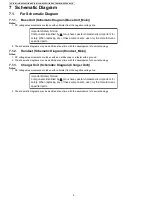
7 Schematic Diagram

7.1.

For Schematic Diagram

7.1.1.

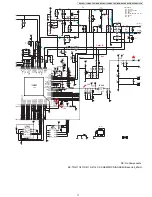
Base Unit (Schematic Diagram (Base Unit_Main))

Notes:

1. DC voltage measurements are taken with voltmeter from the negative voltage line.

2. The schematic diagrams may be modified at any time with the development of new technology.

7.1.2.

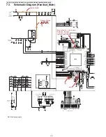
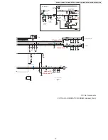
Handset (Schematic Diagram (Handset_Main))

Notes:

1. DC voltage measurements are taken with an oscilloscope or a tester with a ground.
2. The schematic diagrams may be modified at any time with the development of new technology.

7.1.3.

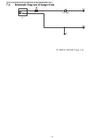
Charger Unit (Schematic Diagram (Charger Unit))

Notes:

1. DC voltage measurements are taken with voltmeter from the negative voltage line.

2. The schematic diagrams may be modified at any time with the development of new technology.

Important Safety Notice:
Components identified by      mark have special characteristics important for
safety. When replacing any of these components, use only the manufacture's
specified parts.

Important Safety Notice:
Components identified by      mark have special characteristics important for
safety. When replacing any of these components, use only the manufacture's
specified parts.

Содержание KX-TG4111CB

Страница 1: ...o 6 KX TG4112 1 TG4111 2 TGA410 1 Up to 6 KX TG4113 1 TG4111 3 TGA410 2 Up to 6 KX TG4114 1 TG4111 4 TGA410 3 Up to 6 KX TGA410 1 TGA410 1 Configuration for each model Information for optional accessories You can expand your phone system by registering optional handsets KX TGA660C KX TGA659C to a single base unit Optional handsets and the supplied handset are different model so that some functions...

Страница 2: ... in the Schematic Diagrams Circuit Board Diagrams Exploded Views and Replacement Parts List It is essential that these critical parts should be replaced with manufacturer s specified parts to prevent shock fire or other hazards Do not modify the original design without permission of manufacturer IMPORTANT INFORMATION ABOUT LEAD FREE PbF SOLDERING If lead free solder was used in the manufacture of ...

Страница 3: ...out Lead Free Solder PbF Pb free 4 2 3 Discarding of P C Board 5 3 Specifications 6 4 Location of Controls and Components 7 5 Installation Instructions 7 6 Operating Instructions 7 7 Schematic Diagram 8 7 1 For Schematic Diagram 8 7 2 Schematic Diagram Base Unit_Main 10 7 3 Schematic Diagram Handset_Main 12 7 4 Schematic Diagram Charger Unit 14 8 Exploded View and Replacement Parts List 15 ...

Страница 4: ...ries according to the instructions 2 2 About Lead Free Solder PbF Pb free Note In the information below Pb the symbol for lead in the periodic table of elements will refer to standard solder or solder that contains lead We will use PbF solder when discussing the lead free solder used in our manufacturing process which is made from Tin Sn Silver Ag and Copper Cu This model and others like it manufa...

Страница 5: ...d Bismuth Sn Zn Bi Please check the manufacturer s specific instructions for the melting points of their products and any precautions for using their product with other materials The following lead free PbF solder wire sizes are recommended for service of this product 0 3 mm 0 6 mm and 1 0 mm 2 3 Discarding of P C Board When discarding P C Board delete all personal information such as telephone di...

Страница 6: ...air humidity dry Approx 77 mm 126 mm 90 mm Approx 140 g Rechargeable Ni MH battery AAA R03 size 1 2 V 550 mAh Super Heterodyne PLL synthesizer Quadrature Discriminator 13 824 MHz 100 Hz Frequency Modulation 40 bit Tone DTMF Pulse Up to 48 digits Up to 24 digits Phonebook 11 days at Standby 13 hours at Talk 0 C 40 C 32 F 104 F 20 80 relative air humidity dry Approx 159 mm 49 mm 29 mm Approx 130 g B...

Страница 7: ...efer to the Operating Instructions Instruction book on TSN Server 5 Installation Instructions Refer to the Operating Instructions Note You can download and refer to the Operating Instructions Instruction book on TSN Server 6 Operating Instructions Refer to the Operating Instructions Note You can download and refer to the Operating Instructions Instruction book on TSN Server ...

Страница 8: ...e schematic diagrams may be modified at any time with the development of new technology 7 1 3 Charger Unit Schematic Diagram Charger Unit Notes 1 DC voltage measurements are taken with voltmeter from the negative voltage line 2 The schematic diagrams may be modified at any time with the development of new technology Important Safety Notice Components identified by mark have special characteristics...

Страница 9: ...9 KX TG4111CB KX TG4112CN KX TG4113CB KX TG4114CB KX TGA410CB KX TGA410CN Memo ...

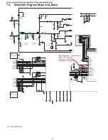
Страница 10: ...DA801 1 2 3 GND C516 0 1u C805 2 7p GND TXON R806 470 RXp LCD_CS LCD_VDD LCD_RST LCD_CD LCD_SCL LCD_SIO LCD_GND WBX02 AP1 10pin PARALLEL WIRE R502 33 TCK URX TDI RTCK TMS UTX TDO UGND C670 NC WBX01 AP1 10pin PARALLEL WIRE C652 NC SW1 LOCATOR 1 2 NC KEYIN2 KEYS_C C660 NC KEYS_D C653 NC KEYS_E C654 NC ANS_LED MSG_LED LED_VDD VBAT C655 NC KEYIN3 KEYIN1 C656 NC C651 NC L661 NC L662 NC L663 NC L664 NC ...

Страница 11: ...1u HAK_CL1 C142 K0 01u L474 NC C165NC C115 NC C164 NC RA504 68 1 2 3 4 C504 1u C185 NC R151 100k C181 NC L1T C507 K2 2u 3 0V R172 100k Q141 B E C 3 0V CHARGE C514 0 1u 5 5V C331 NC R331 68k C351 1u VBG C110 NC C114 NC R115 NC R511 NC R510 10k C341 330u 6 3 C306 100u SA103 NC 2 1 3 IN 2 OUT1 1 ADJ 4 OUT2 D142 30V AK Q111 B C E Q171 B C E D133 A K D153NC A K D113 A K D361 NC AK C161 10u C511 10u C50...

Страница 12: ... DOWN UP LEFT RIGHT 4 0V IC4 NC 1 VOUT 2 GND 4 CN 5 VCC 3 SHD 6 CP C58 NC VBAT R562 NC 3 0V 4 0V R563 0 C2 220u 6 3 C10 220u 6 3 C1 220u 6 3 Q9 C150 0 1u C23 0 1u C24 1u C188 1u C32 1u C84 NC GND L6 NC C34 39p Q2 C19 1000p Q3 R9 30k R8 3 3 R2 30k Q4 R6 10k CN3_C 5 A0 CN3_C 2 OTP_PWR CN3_C 9 VDDA CN3_C 3 CS1 CN3_C 12 GND CN3_C 11 V0 CN3_C 7 SI CN3_C 6 SCL CN3_C 4 RES CN3_C 10 VSS CN3_C 8 VDD CN3_C ...

Страница 13: ... C814 NC ZA1 NC C98 NC C99 NC GND GND C896 1 8p C805 2 4p C806 2 4p C810 2 5p C813 1 6p C812 8 2n L809 1p C811 100p C822 10p C826 10p C825 10p C897 24p C37 10u R35 100k 3 0V X1 13 824M C73 10p C72 10p GND GND L13 180n L14 NC C86 22u L9 0 R28 2 2k GND ANT_TP MIC AP1 1 2 ANT Short GND ANT Short R10 10 D21 4 3V D14 4 3V D13 4 3V D22 4 3V MIC POWER RECEIVER RECEIVER W 0 2mm L 3 8mm 1st layer Test Patt...

Страница 14: ...14 KX TG4111CB KX TG4112CN KX TG4113CB KX TG4114CB KX TGA410CB KX TGA410CN 7 4 Schematic Diagram Charger Unit J1 2 1 G TP1 TP2 F1 R1 6 8 2W SCHEMATIC DIAGRAM Charger Unit ...

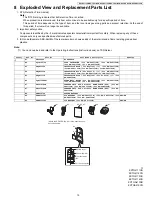
Страница 15: ... KXTG4112CN KXTG4113CB KXTG4114CB KXTGA410CB KXTGA410CN Safety Ref No Part No Part Name Description Remarks A1 PNLV226Z AC ADAPTOR A2 PQJA10075Z CORD TELEPHONE for KX TG4111CB for KX TG4112CN for KX TG4113CB for KX TG4114CB A3 PNQX3129Z INSTRUCTION BOOK for English 1 for KX TG4111CB for KX TG4112CN for KX TG4113CB for KX TG4114CB A4 PNQX3130Z INSTRUCTION BOOK for French 1 for KX TG4111CB for KX TG...

Отзывы: