background image

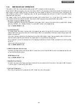
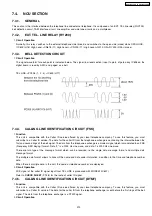
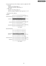
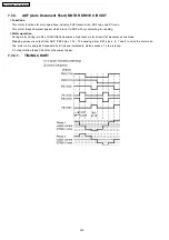
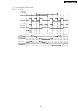
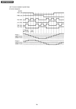
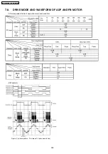
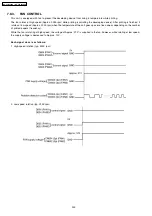
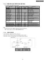
7.7.2.1. TIMING CHART

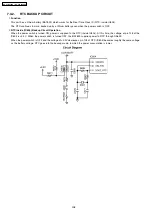
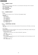
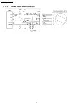
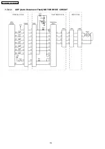
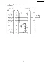
7.7.2. ADF (Auto Document Feed) MOTOR DRIVE CIRCUIT

 1. 

Functions

This motor functions for main operations including FAX transmission, ADF copy and PC scan.

This motor feeds document papers which are set to ADF with synchronizing for reading.

 2. 

Motor operation

During motor driving, pin 98 of ASIC IC604 becomes a high level, motor driver IC51 becomes active mode.

Stepping pulses are output from ASIC IC604 pins, 100 ~ 105 causing driver IC51 pins 4, 6, 7 and 9 to drive the motor coil.

The motor coil is energized sequentially in 2 phase increments, which causes a 1-step rotation.

A 1-step rotation feeds 0.042mm of document paper.

222

KX-FLB852CX / KX-FLB852CXS

Содержание KX-FLB852CX

Страница 1: ... law KX FLB852CX KX FLB852CXS KX FA101E KX FA101A Optional Lower Input Tray KX FA102E KX FA102A Optinal LAN Board KX FA104E Maintenance Kit for Asia Middle Near East South America and Africa for Singapore Soudi Arabia Asia Middle Near East All in One Flatbed Laser Fax with Multi Action Sorter ORDER NO KMF0602928CE ...

Страница 2: ...TI ROLLER SECTION PARTS 67 5 22 REMOVE THE OPERATION PANEL 68 5 23 REMOVE THE SCANNER COVER 69 5 24 REMOVE THE SCANNER SECTION PARTS 70 5 25 REMOVE THE FUSER UNIT AND LOWER GLASS 71 5 26 REMOVE THE FUSER UNIT PARTS 72 5 27 NOTE FOR ASSEMBLING 73 5 28 INSTALLATION POSITION OF THE LEAD 75 6 TROUBLESHOOTING GUIDE 81 6 1 USER RECOVERABLE ERRORS 81 6 2 PROGRAMMING AND LISTS 84 6 3 TEST FUNCTIONS 88 6 4...

Страница 3: ...SOR BOARD PARTS 328 12 14 THERMISTOR BOARD PARTS 328 12 15 RELAY BOARD PARTS 328 12 16 VARISTOR BOARD PARTS 328 12 17 REGISTRATION SENSOR BOARD PARTS 328 12 18 HIGH VOLTAGE POWER BOARD 328 12 19 LOW VOLTAGE POWER BOARD 329 12 20 LAN BOARD PARTS OPTION 330 12 21 HOOK SWITCH BOARD OPTION 331 12 22 CASSETTE RELAY BOARD PARTS OPTION 331 12 23 PAPER SWITCH BOARD PARTS OPTION 331 12 24 COVER SWITCH BOAR...

Страница 4: ... 10 C In case of using high temperature soldering iron please be careful not to heat too long PbF solder will tend to splash if it is heated much higher than its melting point approximately 1100 F 600 C When applying PbF solder to double layered boards please check the component side for excess which may flow onto the opposite side See figure below 1 1 1 SUGGESTED PBF SOLDER There are several type...

Страница 5: ...me etc Note Some exposed parts may be isolated from the chassis by design These will read infinity 4 If the measurement is outside the specified limits there is a possibility of a shock hazard 1 4 FOR SERVICE TECHNICIANS ICs and LSIs are vulnerable to static electricity When repairing the following precautions will help prevent recurring malfunctions 1 Cover the plastic part s boxes with aluminum ...

Страница 6: ...SECTIONS OF THE UNIT Be careful not to let your hair clothes fingers accessories etc become caught in any moving sections of the unit The moving sections of the unit are the rollers and a gear There is a separation roller and a document feed roller which are rotated by the document feed motor A gear rotates the two rollers Be careful not to touch them with your hands especially when the unit is op...

Страница 7: ...wer supply unit Therefore always unplug the AC power cord before disassembling for service 1 7 3 LASER BEAM AND FUSER UNIT SECTION The printer of this unit utilizes a laser Use of controls or adjustments or performance of procedures other than those specified herein may result in hazardous radiation exposure The fuser unit is inside of the unit and gets hot Do not touch it when removing the jammed...

Страница 8: ...rson For instance clothes rubbing together can damage electric elements or change their electrical characteristics In order to prevent static electricity touch a metallic part that is grounded to release the static electricity Never touch the electrical sections such as the power supply unit etc 8 KX FLB852CX KX FLB852CXS ...

Страница 9: ...ed characters FINE For originals with small printing SUPER FINE For originals with very small printing PHOTO For originals containing photographs shaded drawing etc Broad cast 250 sheet paper capacity 60 g m2 75 g m2 16 lb 20 lb Distinctive ring detection Sorter Large Memory Performed by DRAM Approx 150 pages of memory transmission Approx 630 pages of memory reception Phone Line Monitor On hook di...

Страница 10: ... Approx 75 W Transmission Approx 28 W Reception Approx 400 W Copy Approx 430 W Maximum Approx 900 W When the fuser lamp turns on Power Supply 220 240 V AC 50 60 Hz Fax Memory Capacity 10 MB in total Approx 630 pages of memory reception with back up Max 255 pages per one reception Approx 150 pages of memory transmission Based on the ITU T No 1 Test Chart in standard resolution Laser diode propertie...

Страница 11: ...64 MB or more Windows XP 1 128 MB or more Other Hardware CD ROM drive Hard disk drive with at least 100 MB of available space USB interface LAN interface for optional LAN board 10BASE T 100BASE TX 1 Multi Function Station software does not work with Windows XP Professional x64 Edition 64bit a new version of Windows XP Professional that was released in and after April 2005 2 4 OPTIONAL ACCESSORIES ...

Страница 12: ...ng paper exit 12 Output tray 1 Power switch 2 USB interface connector 3 Recording paper guides 4 Multi purpose input tray 5 Power inlet 6 LAN board Optional connector LAN connection jack 10Base T 100Base TX cable 7 Telephone line jack 8 External telephone jack 9 Speaker 10 Handset unitFPFKE 3 INSTALLATION 3 1 LOCATION OF CONTROLS 3 1 1 OVERVIEW 3 1 1 1 Front view 3 1 1 2 Rear view 12 KX FLB852CX K...

Страница 13: ...RY 6 CONTRAST 7 RESOLUTION 8 ZOOM QUICK SCAN 9 MENU 10 CLEAR 11 SORT 12 MANUAL BROAD 13 FAX AUTO ANSWER 14 LOWER 15 FAX 16 COPY 17 SET 18 SCAN 19 Navigator key 20 TONE 21 PAUSE REDIAL 22 FLASH 23 MONITOR 24 START 25 STOP 3 1 2 CONTROL PANEL 13 KX FLB852CX KX FLB852CXS ...

Страница 14: ... machine or an extension telephone Remove the stopper if attached 4 Answering machine not included 5 Handset unit Optional connection jack You can connect the optional handset unit Remove the seal if attached Note To avoid malfunction do not position the unit near appliances such as TVs or speakers which generate an intense magnetic field If any other device is connected to the same telephone line...

Страница 15: ...ications for Microsoft Windows that support TWAIN scanning Storing editing or erasing entries in directories using your computer Programming the features using your computer Sending receiving fax documents using your computer To use Multi Function Station on your computer the following are required Operating System Works with Windows 98 Me 2000 XP 1 CPU Windows 98 Pentium 90 MHz or faster Windows ...

Страница 16: ...ust be purchased separately Be sure to use a Hi Speed USB 2 0 certified cable if your computer is equipped with the Hi Speed USB 2 0 interface Refer to EXTENSION USB CABLE KIT P 332 3 2 4 Connecting to the LAN For example connect the fax unit as shown below 16 KX FLB852CX KX FLB852CXS ...

Страница 17: ...meters 16 4 feet Using a longer cord may reduce the voltage or cause malfunctions Avoid direct sunlight Do not install near devices which contain magnets or generate magnetic fields Do not subject the unit to strong physical shock or vibration Keep the unit clean Dust accumulation can prevent the unit from functioning properly To protect the unit from damage hold both sides when you move it Do not...

Страница 18: ...computer set the printer properties 3 3 3 1 Attaching the tray label Attach the tray label 1 to the output tray 2 Label 1 to the upper output tray 1 Label 2 to the middle output tray 2 Label 3 to the lower output tray 3 Note Instead of the label 1 2 3 you can also attach other labels for print copy or fax according to the usage For a blank label this is convenient if the optional LAN board is inst...

Страница 19: ...n area where the output tray may be easily bumped into The upper output tray can hold up to approximately 100 sheets of printed paper The other output trays can hold up to approximately 50 sheets of printed paper Remove the printed paper before the output tray becomes full 19 KX FLB852CX KX FLB852CXS ...

Страница 20: ...letter or legal size paper change the setting Refer to PROGRAM MODE TABLE P 97 by using PAPER TRAY in the copy mode in feature 380 1 Pull open the paper input tray 1 2 Pinch the right side of the recording paper guide 1 then slide it to match the paper size mark Pinch the front side of the recording paper guide 2 then slide it open to its full width 3 Before loading a stack of paper fan the paper ...

Страница 21: ...not close the plate in the paper input tray may be lifted Push the paper and check that the paper is flat in the paper input tray To pull the paper input tray completely out Pull the paper input tray 1 until it clicks into place then pull it completely out lifting the front part of the tray To insert the paper input tray Insert the paper input tray 1 to the unit lifting the front part of the tray ...

Страница 22: ...y setting for faxing feature 440 input tray setting for copying feature 460 To use the optional input tray with your computer you need to change the printer properties 3 3 4 2 Using the multi purpose input tray A4 letter or legal size recording paper can be used The multi purpose input tray can hold Up to 30 sheets of 60 g m2 to 75 g m2 paper Up to 30 sheets of 80 g m2 paper Up to 25 sheets of 90 ...

Страница 23: ...to the size of the recording paper The paper should not be over the tabs 2 If the paper is not inserted correctly readjust the paper or the paper may jam 3 3 4 3 Checking the amount of remaining recording paper The paper level indicator green will allow you to check the amount of remaining paper The paper is full 1 The paper is empty 2 23 KX FLB852CX KX FLB852CXS ...

Страница 24: ...nsert the tab 1 into the slot 2 on the unit and insert the rib 3 of the handset cradle into the bottom groove 4 of the speaker Make sure that the triangles 1 match to install the handset unit correctly 1 Pull the handset unit slightly forward 1 and then remove the rib of the handset cradle by lifting the handset unit in the direction of the arrow 2 24 KX FLB852CX KX FLB852CXS ...

Страница 25: ... Do not set the following types of documents Make a copy of the document and send the copy Chemically treated paper such as carbon or carbonless duplicating paper Electrostatically charged paper Badly curled creased or torn paper Paper with a coated surface Paper with printing on the opposite side that can be seen through the other side such as newsprint 3 3 6 2 Using the scanner glass Effective s...

Страница 26: ...ss and set the copy Remove clips staples or other fasteners when using the auto document feeder Do not set the following types of documents when using the auto document feeder Make a copy of the document using the scanner glass and set the copy instead Chemically treated paper such as carbon or carbonless duplicating paper Electrostatically charged paper Badly curled creased or torn paper Paper wi...

Страница 27: ...3 3 7 TO SELECT CHARACTERS WITH THE DIAL KEYPAD Pressing the dial keys will select a character as shown below 3 3 8 TO SELECT CHARACTERS USING OR 27 KX FLB852CX KX FLB852CXS ...

Страница 28: ...3 3 9 SETTING YOUR LOGO The logo can be your name or the name of your company 28 KX FLB852CX KX FLB852CXS ...

Страница 29: ...onic toner cartridge and drum unit The drum unit contains a photosensitive drum Exposing it to light may damage the drum Once you have opened the protection bag Do not expose the drum unit to light for more than 5 minutes Do not touch or scratch the black drum surface Do not place the drum unit near dust or dirt or in a high humidity area Do not expose the drum unit to direct sunlight Do not turn ...

Страница 30: ... cartridge and the drum unit at the same time skip to step 7 5 Turn the two green levers 1 on the used toner cartridge firmly 6 Remove the used cartridge 1 from the drum unit 2 The toner may stick to the cartridge and the drum unit Be careful when handling Do not drop the toner on the black drum surface 3 Put the used toner cartridge into the protection bag 30 KX FLB852CX KX FLB852CXS ...

Страница 31: ...idge 1 into the drum unit 2 8 Firmly press down the toner cartridge to snap into position 9 Turn the two green levers 1 on the toner cartridge firmly 10 Make sure that the triangles 1 match to install the toner cartridge correctly If the lower glass 2 is dirty clean it with a soft and dry cloth 31 KX FLB852CX KX FLB852CXS ...

Страница 32: ...r 1 Then push down the right centre edge until locked Caution To prevent injuries be careful not to put your hands under the top cover Note While the unit displays PLEASE WAIT do not open the top cover or turn the power switch OFF Waste disposal method Waste material should be disposed of under conditions which meet all national and local environmental regulations 32 KX FLB852CX KX FLB852CXS ...

Страница 33: ...not sure what the drive letter is for your CD ROM drive use Windows Explorer and look for the CD ROM drive The installation will start 3 When the setup program starts follow the on screen instructions 4 When the Setup Type dialog box appears select Standard then click Next Readiris OCR software and Device Monitor will also be installed 5 When the Connect Type dialog box appears select Connect dire...

Страница 34: ...ng to determine if the problem originates from the transmitter receiver or the telephone line 4 Determine causes Determine the causes of the equipment problem by troubleshooting 5 Equipment repairs Repair or replace the defective parts and take appropriate measures at this stage to ensure that the problem will not recur 6 Confirm normal operation of the equipment After completing the repairs condu...

Страница 35: ...er No Item Cleaning Cycle Replacement Cycle Procedure 1 ADF Document Feed Roller Ref No 151 3 months 7 years 100 000 documents Refer to REMOVE THE ADF PARTS 2 P 58 2 ADF Separation Rubber Ref No 141 3 months 7 years 100 000 documents Refer to REMOVE THE ADF PARTS 1 P 57 3 ADF Eject Roller Ref No 173 3 months 7 years 100 000 documents Refer to REMOVE THE ADF PARTS 2 P 58 4 Pick up Roller Ref No 269...

Страница 36: ...er density When the unit has printed 80 000 pages following message will appear to tell the time for replacement Provided that the following symptoms are found we recommend that you replace the above mentioned maintenance kit all together 4 1 3 2 Symptoms that happen in each maintenance kit when replacement is required 4 1 3 2 1 Fuser unit Paper often jams inside the fuser unit Paper twines around...

Страница 37: ...LER STANDARD then the roller starts feeding paper When paper is fed manually the plunger of solenoid is pulled to drive PICK UP ROLLER MULTI then the roller starts feeding paper When paper is fed from the optional cassette first the optional cassette motor OPTION MOTOR starts to rotate the plunger of solenoid is pulled to drive PICK UP ROLLER OPTION CASSETTE then the roller starts feeding paper 37...

Страница 38: ...d paper is separated by ROLLER DOC SEPARATION and RUBBER SEPARATION and then fed by ROLLER DOC FEED After being read by CCD the paper is discharged by ROLLER DOC EJECT DOCUMENT TRANSMISSION SCANNER GLASS CCD Module is carried by the belt timing along the shaft carriage to the reading start position Then it goes back to the home position reading the document through the glass 38 KX FLB852CX KX FLB8...

Страница 39: ...arty Caution Be careful when handling the drum and toner unit Do not use paper products such as paper towels or tissues to clean the inside of the unit 4 4 1 1 White plate and scanner glasses 1 Turn the power switch OFF 2 Hold the ADF cover 1 firmly and lift it to open the upper part 2 of the ADF cover then open the whole of the ADF cover 3 Clean the scanner glass 1 and the white cover sheet 2 and...

Страница 40: ...5 Close the document cover 1 6 Turn the power switch ON If the document cover comes off from the unit 1 Attach the hinges 1 to the document cover 2 Make sure that the inserted direction is correct Otherwise the hinges cannot be inserted into the slots in step 3 2 Lay down the hinges 1 40 KX FLB852CX KX FLB852CXS ...

Страница 41: ...ver 4 4 1 2 Lower glass 1 Turn the power switch OFF 2 Lift the top cover release lever 1 and open the top cover 2 Important Close the multi purpose input tray 3 before opening the top cover 3 Remove the drum and toner unit 1 by holding the two tabs 41 KX FLB852CX KX FLB852CXS ...

Страница 42: ...ure that the triangles 2 match to install the drum and toner unit correctly 6 Close the top cover holding the cover release lever 1 Then push down the right centre edge until locked Caution To prevent injuries be careful not to put your hands under the top cover 7 Turn the power switch ON 42 KX FLB852CX KX FLB852CXS ...

Страница 43: ...ft it to open the upper part 2 of the ADF cover then open the whole of the ADF cover 3 Clean the document feeder rollers 1 with a cloth moistened with isopropyl rubbing alcohol and let all parts dry thoroughly Clean the rollers in the direction of the arrow to avoid the discharge brush 2 from being pulled 4 Close the ADF cover 5 Turn the power switch ON 43 KX FLB852CX KX FLB852CXS ...

Страница 44: ...he ADF cover 1 Hold the ADF cover 1 firmly and lift it to open the upper part 2 of the ADF cover then open the whole of the ADF cover 2 Remove the jammed document 1 carefully When the document has jammed near the document entrance When the document has jammed near the document exit 44 KX FLB852CX KX FLB852CXS ...

Страница 45: ... recording paper has jammed inside of the unit The display will show the following Caution Do not pull out the jammed paper forcibly before opening the top cover To prevent injuries be careful not to put your hands under the top cover 45 KX FLB852CX KX FLB852CXS ...

Страница 46: ...se input tray 3 before opening the top cover 2 Remove the jammed paper Case 1 When the recording paper has jammed near the drum and toner unit Remove the jammed paper 1 carefully by pulling it upwards Remove the jammed paper 1 carefully by pulling it to the right 46 KX FLB852CX KX FLB852CXS ...

Страница 47: ... 1 until they stop 2 Remove the jammed paper 1 carefully by pulling it upwards 3 Push back the green levers 1 to the original position Case 3 When the recording paper has jammed near the output tray 1 Pull and hold the green lever 1 to release the jammed paper 47 KX FLB852CX KX FLB852CXS ...

Страница 48: ...2 Remove the jammed paper 1 carefully by pulling it upwards 3 Close the top cover holding the cover release lever 1 Then push down the right centre edge until locked 48 KX FLB852CX KX FLB852CXS ...

Страница 49: ...splay will show the following 1 Open the cover 1 at the left side of the optional tray Caution Do not pull the option tray before opening the cover 2 Remove the jammed paper 1 3 Close the cover at the left side of the optional input tray 49 KX FLB852CX KX FLB852CXS ...

Страница 50: ...l show the following 1 Pull open the input tray then remove the recording paper and straighten 2 Re load the recording paper Paper input tray Optional input tray 3 Close the input tray Note If the error message is still displayed check the recording paper specifications and re install recording paper 50 KX FLB852CX KX FLB852CXS ...

Страница 51: ...to the unit properly The display will show the following 1 Remove the recording paper and straighten 2 Re insert the recording paper Note If the error message is still displayed check the recording paper specifications and re install recording paper 51 KX FLB852CX KX FLB852CXS ...

Страница 52: ...5 DISASSEMBLY INSTRUCTIONS Note Remove the Document Cover the Paper Input tray and the drum and toner cartridge before reassembling 52 KX FLB852CX KX FLB852CXS ...

Страница 53: ...5 1 LOWER CABINET SECTION 53 KX FLB852CX KX FLB852CXS ...

Страница 54: ...5 2 PRINTER COVER SECTION 54 KX FLB852CX KX FLB852CXS ...

Страница 55: ...5 3 ADF SECTION 5 4 INNER CABINET SECTION 55 KX FLB852CX KX FLB852CXS ...

Страница 56: ...5 5 REMOVE THE ADF UNIT 56 KX FLB852CX KX FLB852CXS ...

Страница 57: ...5 6 REMOVE THE ADF PARTS 1 57 KX FLB852CX KX FLB852CXS ...

Страница 58: ...5 7 REMOVE THE REAR PANEL 5 8 REMOVE THE ADF PARTS 2 58 KX FLB852CX KX FLB852CXS ...

Страница 59: ...5 9 REMOVE THE BOTTOM PLATE 5 10 REMOVE THE ANALOG BOARD 59 KX FLB852CX KX FLB852CXS ...

Страница 60: ...5 11 REMOVE THE HVPS FAN TERMINAL UNIT 5 12 REMOVE THE CASSETTE GUIDE AND THE RELAY BOARD 60 KX FLB852CX KX FLB852CXS ...

Страница 61: ...5 13 REMOVE THE DIGITAL BOARD 5 14 REMOVE THE LASER UNIT AND THE SHUTTER 61 KX FLB852CX KX FLB852CXS ...

Страница 62: ...5 15 REMOVE THE REAR CABINET PARTS 62 KX FLB852CX KX FLB852CXS ...

Страница 63: ...5 16 REMOVE THE PRINTER COVER 63 KX FLB852CX KX FLB852CXS ...

Страница 64: ...5 17 REMOVE THE GEAR CHASSIS AND GEAR SECTION 64 KX FLB852CX KX FLB852CXS ...

Страница 65: ...5 18 REMOVE THE LOWER PRINTER COVER PARTS 65 KX FLB852CX KX FLB852CXS ...

Страница 66: ...5 19 REMOVE THE MULTI ROLLER SECTION 66 KX FLB852CX KX FLB852CXS ...

Страница 67: ...5 20 REMOVE THE SEPARATION RUBBER MULTI ROLLER 5 21 REMOVE THE MULTI ROLLER SECTION PARTS 67 KX FLB852CX KX FLB852CXS ...

Страница 68: ...5 22 REMOVE THE OPERATION PANEL 68 KX FLB852CX KX FLB852CXS ...

Страница 69: ...5 23 REMOVE THE SCANNER COVER 69 KX FLB852CX KX FLB852CXS ...

Страница 70: ...5 24 REMOVE THE SCANNER SECTION PARTS 70 KX FLB852CX KX FLB852CXS ...

Страница 71: ...5 25 REMOVE THE FUSER UNIT AND LOWER GLASS 71 KX FLB852CX KX FLB852CXS ...

Страница 72: ...5 26 REMOVE THE FUSER UNIT PARTS 72 KX FLB852CX KX FLB852CXS ...

Страница 73: ...ER CABINET SECTION When assembling place the Main Unit as shown below to avoid any damage on the unit 5 27 2 FUSER UNIT After servicing a Fuser Unit clean the 10 Ribs so as not to rub off the ink on the paper 73 KX FLB852CX KX FLB852CXS ...

Страница 74: ...5 27 3 OPERATION BOARD When removing the Operation Board you need to release the Lead from the Boss in advanced 5 27 4 FB SECTION 74 KX FLB852CX KX FLB852CXS ...

Страница 75: ...5 28 INSTALLATION POSITION OF THE LEAD 5 28 1 ADF SECTION 1 5 28 2 ADF SECTION 2 75 KX FLB852CX KX FLB852CXS ...

Страница 76: ...5 28 3 PRINTER COVER INNER 76 KX FLB852CX KX FLB852CXS ...

Страница 77: ...5 28 4 PRINTER COVER BOTTOM 77 KX FLB852CX KX FLB852CXS ...

Страница 78: ...5 28 5 BOTTOM SECTION 1 78 KX FLB852CX KX FLB852CXS ...

Страница 79: ...5 28 6 BOTTOM SECTION 2 79 KX FLB852CX KX FLB852CXS ...

Страница 80: ...5 28 7 REAR SECTION 80 KX FLB852CX KX FLB852CXS ...

Страница 81: ...rrectly Pull the input tray out then reinsert it The memory telephone numbers parameters etc has been erased Re program 1 Paper input tray 2 Multi purpose input tray 3 Optional input tray Recording paper was not fed into the unit properly Re insert the recording paper The cover at the left side of the optional input tray is open Close it The ADF cover is open Close it There is no space to store ne...

Страница 82: ...has been fully stacked on the output tray Remove the stacked paper A recording paper jam occurred inside of the optional input tray Clear the jammed paper A recording paper jam occurred inside of the optional input tray Clear the jammed paper The cable or the computer power cord is not connected correctly Check the connections The software is not running on the computer Restart the software and tr...

Страница 83: ...r is open Close it A transmission error occurred Try again The inside of the unit is too cold Let the unit warm up Wait for a while The unit is warming up before operation starts Wait for a while The fax message was printed on paper which is shorter than A4 size paper Use the appropriate size paper 83 KX FLB852CX KX FLB852CXS ...

Страница 84: ...d in the Operating Instructions and are available to the user The special programs are only those listed here and not displayed to the user In both the User and Service Modes there are Set Functions and Test Functions The Set Functions are used to program various features and functions and the Test Functions are used to test the various functions The Set Functions are accessed by entering their co...

Страница 85: ...izer select 1 0 km 2 1 8 km 3 3 6 km 4 7 2 km 1 4 1 Set RX equalizer to automatic mode 524 Transmission equalizer select 1 0 km 2 1 8 km 3 3 6 km 4 7 2 km 1 4 1 529 Call Service Clear 550 Memory clear Refer to Memory Clear Specification P 87 551 ROM check See P 88 552 DTMF single tone test 1 ON 2 OFF 1 2 2 See P 88 553 Monitor on FAX communication select 1 OFF 2 PHASE B 3 ALL 1 3 1 Sets whether to...

Страница 86: ...3 See P 111 670 Update the number of maintenance 1 Change maintenance kit 0 1 When 670 is entered the setting value is not displayed Press Set key and the unit rings a beep sound and the number of maintenance kit exchange record is increased 710 Memory clear except History data Refer to Memory Clear Specification P 87 717 Transmit speed selection 1 14400BPS 2 12000BPS 3 9600BPS 4 7200BPS 5 4800BPS...

Страница 87: ... 550 when you want to reset the all setting data keeping the user information 2 Execute Service Mode 710 to clear the user information in case that Main Unit is recycled Note Please restart a power supply after clearing a memory 87 KX FLB852CX KX FLB852CXS ...

Страница 88: ...1 V34 26400bps 22 V34 28800bps 23 V34 31200bps 24 V34 33600bps 25 1100Hz 22 2100Hz SET ROM CHECK Service Mode 5 5 1 Indicates the version and checks the sum of the ROM SET LCD CHECK Service Mode 5 5 8 Checks the LCD indication Illuminates all the dots to check if they are normal SET DTMF SINGLE TEST Service Mode 5 5 2 Outputs the DTMF as single tones Used to check the frequencies of the individual...

Страница 89: ... A ADF cover A Cover open Cover close H Home H CCD at Home position CCD not at Home position None M Manual paper M Paper set No paper None 1 Sorter bin1 1 Paper detect No paper 2 Sorter bin2 2 Paper detect No paper 3 Sorter bin3 3 Paper detect No paper None C Option cassette paper tray or cover C Cover open Cover close P Option cassette paper P Paper set No paper U Option casette pickup U Paper de...

Страница 90: ...s to be input for the various test modes 6 3 1 DTMF SINGLE TONE TRANSMIT SELECTION Note After performing this check do not forget to turn the setting off otherwise dialing in DTMF signal will not work 6 3 2 BUTTON CODE TABLE 90 KX FLB852CX KX FLB852CXS ...

Страница 91: ...se print test patterns are just image printing and different from actual ones When it is required to judge the print quality compare with the printing of a nondefective machine 6 3 3 PRINT TEST PATTERN 91 KX FLB852CX KX FLB852CXS ...

Страница 92: ...nect the USB cable to USB hub connect it to the USB port of your computer directly Make sure you have installed the latest Service Pack available for the version of Windows installed on your computer See the Microsoft web site for details Confirm the BIOS setting of your computer and select USB port mode Please refer to your computer operating instructions or consult the manufacturer If you have a...

Страница 93: ... connection Disable the firewall software or change the firewall setting to work Multi Function Station properly I cannot enter the following feature code on the fax unit 443 490 491 492 500 501 502 503 507 Make sure the LAN board has been attached correctly I cannot find the fax unit in the Target Device or Device Select dialog box when operating the following functions PC scan Remote Control PC ...

Страница 94: ...ocking the connection and the setup program may not list any fax units Consult your network administrator and temporarily disable the firewall software The Windows Security Alert dialog box appears and asks if you want to block PCCMFLPD and I cannot operate the following functions after installing the Microsoft Windows XP Service Pack 2 PC printing PC scan Remote Control PC FAX Device Monitor Clic...

Страница 95: ...rvice list code 999 from the customer s fax machine Based on this the parameters for the desired codes can be changed The procedure for changing and listing parameters is described on ENTERING THE REMOTE PROGRAMMING MODE AND CHANGING SERVICE CODES P 96 Also before exiting the remote programming mode it is advisable to obtain a new list to confirm that the changes were made correctly Hint Since the...

Страница 96: ...6 5 1 ENTERING THE REMOTE PROGRAMMING MODE AND CHANGING SERVICE CODES CROSS REFERENCE PROGRAM MODE TABLE P 97 96 KX FLB852CX KX FLB852CXS ...

Страница 97: ... AUTO PRINT 1 ON 2 OFF ON OK 404 MANUAL ANSWER MODE 1 TEL 0 TEL FAX TEL 411 OVERSEAS MODE 1 NEXT FAX 2 ERROR 0 OFF ERROR OK 412 DELAYED SEND 1 ON 2 OFF OFF NG 413 ECM SELECTION 1 ON 2 OFF ON OK 416 CONNECTING TONE 1 ON 2 OFF ON OK 430 DISTINCTIVE RING 1 ON 2 OFF OFF OK 431 FAX RING PATTERN B D A B C D B D OK 432 AUTO REDUCTION 1 ON 2 OFF ON OK 434 Remote FAX activation code 1 ON 2 OFF ON CODE 9 NG...

Страница 98: ...communication 1 OFF 2 Phase B 3 ALL OFF OK 554 Modem test NG 556 Motor test H V P S check NG 557 LED test NG 558 LCD test NG 561 Key test NG 563 CCD position adjustment setting 1 31 3 75mm 3 75mm 0 25mm unit 16 NG 564 CCD auto adjustment NG 571 ITS auto redial time set 00 99 03 OK 572 ITS auto redial line disconnection time set 001 999sec 65 OK 573 Remote turn on ring number 01 99 10 OK 574 DIAL T...

Страница 99: ... copying 10 60 20 OK 991 Setup list 1 Start OK 994 Journal list 1 Start OK 995 Journal 2 list 1 Start OK 996 Journal 3 list 1 Start OK 998 History list 1 Start OK 999 Service list 1 Start OK OK means can set NG means can not set Note Refer to SERVICE FUNCTION TABLE P 85 for descriptions of the individual codes Example If you want to set value in the 401 PRINT CONFIRMATION REPORT press the dial key...

Страница 100: ...6 5 3 USER MODE The list below is an example of the SYSTEM SETUP LIST the unit prints out 100 KX FLB852CX KX FLB852CXS ...

Страница 101: ...Note The above values are the default values 6 5 4 SERVICE MODE SETTINGS Example of a printed out list Note The above values are the default values 101 KX FLB852CX KX FLB852CXS ...

Страница 102: ...6 5 5 HISTORY Note See the following descriptions of this report Item No 1 49 are corresponding to the listed items in DESCRIPTIONS OF THE HISTORY REPORT P 103 102 KX FLB852CX KX FLB852CXS ...

Страница 103: ...he user after they purchased the unit 11 USAGE TIME The amount of time the unit has been powered ON 12 FACTORY NOW This shows how many days from factory production until the user prints out this history list 13 TEL MODE The amount of time the TEL mode setting was used 14 FAX MODE The amount of time the FAX mode setting was used 15 Not used 16 Not used 17 FINAL RECEIVE MODE The last set receiving m...

Страница 104: ...a fax message by friendly signal detect 39 Not used 40 RMT DTMF Means the unit detected DTMF Remote Fax activation code entered remotely 41 PAL DTMF Means the unit detected DTMF Remote Fax activation code entered by a parallel connected telephone 42 TURN ON Means the unit started to receive after 10 rings Remote Turn On Service Code 573 43 Not used 44 IDENT Means the unit detected Ring Detection 4...

Страница 105: ...ns for the same problem as they are not a technician or engineer Using your experience test the problem area corresponding to the claim Also returns from a customer or dealer often have a claim tag For these cases as well you need to determine the problem Test the unit using the simple check list on SIMPLE CHECK LIST P 107 Difficult problems may be hard to determine so repeated testing is necessar...

Страница 106: ...alization about 3 seconds and the other is the long initialization about 10 seconds The short initialization makes the unit enter the standby mode The long initialization makes the unit enter the standby mode after cleaning or detecting the rest of toner 106 KX FLB852CX KX FLB852CXS ...

Страница 107: ...6 6 4 SIMPLE CHECK LIST Note Check according to the service code referring to TEST FUNCTIONS P 88 107 KX FLB852CX KX FLB852CXS ...

Страница 108: ...al Failed the high voltage power supply board Go to HIGH VOLTAGE SECTION P 176 Dirty the recording paper path Clean the recording paper path 5 BLACK PRINT P 123 Failed drum unit Replace drum unit Failed LSU Go to LSU SECTION P 170 Failed the high voltage terminal Check the high voltage terminal Failed the high voltage power supply board Go to HIGH VOLTAGE SECTION P 176 Failed the digital board Che...

Страница 109: ...er Dirty or failed the heat roller Clean or replace the heat roller Separator of heat roller a check Replace separator Dust on the recording paper path Clean the recording paper path Failed the paper feed roller Replace the registration roller Failed the pickup sensor lever Check the pickup sensor lever Failed the pickup sensor Go to SENSOR SECTION P 162 Failed the resist sensor lever Check the re...

Страница 110: ...ment guide 3 THE SENT FAX DATA IS SKEWED P 135 The cause of ADF Go to SKEW ADF P 134 The cause of scanner glass Problem with the other FAX machine 4 THE RECEIVED FAX DATA IS SKEWED P 135 The cause of printing Go to SKEW ADF P 134 Problem with the other FAX machine 5 THE RECEIVED OR COPIED DATA IS EXPANDED P 136 Dirty or failed the document feed roller at ADF Clean or replace the document feed roll...

Страница 111: ... after reaching the second stabilizing temperature 205 C 3Ch 05 means that it did not reach the first stabilizing temperature 170 C 5Bh within 30 seconds from detection temperature 1 70 C D8h 06 means that it became 235 C 2Ah or over during printing 07 means that during printing the short of the thermistor AD 00h was detected 08 means that the thermistor s short AD 00h and open AD FFh or over were...

Страница 112: ...6 6 6 1 CALL SERVICE 1 CALL SERVICE 1 means that the polygon motor inside the LSU does not rotate The rotation of the polygon motor is detected by IC604 48pin XREADY 112 KX FLB852CX KX FLB852CXS ...

Страница 113: ...ns that the synchronous signal out of the LSU cannot be detected The synchronous signal out of the LSU is detected by IC 604 59pin XHSYNC Note As for the Pulse waveform of the above flow chart see the timing chart 113 KX FLB852CX KX FLB852CXS ...

Страница 114: ... to or exceed a constant temperature The temperature is monitored with the thermistor inside the fuser and detected with the voltage input into IC 604 21pin When Call Service 3 is occurred the cause can be distinguished by service mode 655 Refer to P 111 for details 114 KX FLB852CX KX FLB852CXS ...

Страница 115: ...unning of the FAN cannot be detected normally The running of the FAN is detected by IC600 16 and 18pin CALL SERVICE 4 is displayed when it detects NG three times continuously After repairing copy three times If CALL SERVICE 4 is displayed check again 115 KX FLB852CX KX FLB852CXS ...

Страница 116: ...116 KX FLB852CX KX FLB852CXS ...

Страница 117: ...6 6 6 5 CALL SERVICE 5 CALL SERVICE 5 means that Main DC motor s rotation detection signal LD does not become Low 117 KX FLB852CX KX FLB852CXS ...

Страница 118: ...6 6 6 6 CALL SERVICE 6 CALL SERVICE 6 indicates that abnormal charge voltage is output from the high voltage unit 118 KX FLB852CX KX FLB852CXS ...

Страница 119: ...6 6 7 PRINT 6 6 7 1 GHOST IMAGE CROSS REFERENCE HIGH VOLTAGE SECTION P 176 POWER SUPPLY BOARD SECTION P 193 119 KX FLB852CX KX FLB852CXS ...

Страница 120: ...6 6 7 2 DARK OR WHITE VERTICAL LINE Note When wiping the cover glass reflecting mirror use a dry and soft cloth 120 KX FLB852CX KX FLB852CXS ...

Страница 121: ...6 6 7 3 DARK OR WHITE HORIZONTAL LINE CROSS REFERENCE HIGH VOLTAGE SECTION P 176 121 KX FLB852CX KX FLB852CXS ...

Страница 122: ...6 6 7 4 DIRTY OR HALF DARKNESS BACKGROUND CROSS REFERENCE HIGH VOLTAGE SECTION P 176 122 KX FLB852CX KX FLB852CXS ...

Страница 123: ...6 6 7 5 BLACK PRINT CROSS REFERENCE HIGH VOLTAGE SECTION P 176 LSU SECTION P 170 123 KX FLB852CX KX FLB852CXS ...

Страница 124: ...6 6 7 6 LIGHT PRINT CROSS REFERENCE HIGH VOLTAGE SECTION P 176 124 KX FLB852CX KX FLB852CXS ...

Страница 125: ...6 6 7 7 BLACK OR WHITE POINT 6 6 8 RECORDING PAPER FEED 6 6 8 1 MULTIPLE FEED 125 KX FLB852CX KX FLB852CXS ...

Страница 126: ...6 6 8 2 THE RECORDING PAPER IS WAVED OR WRINKLED 126 KX FLB852CX KX FLB852CXS ...

Страница 127: ...6 6 8 3 SKEW 127 KX FLB852CX KX FLB852CXS ...

Страница 128: ...6 6 8 4 THE RECORDING PAPER DOES NOT FEED CROSS REFERENCE SENSOR SECTION P 162 MOTOR SECTION P 168 128 KX FLB852CX KX FLB852CXS ...

Страница 129: ...6 6 8 5 THE RECORDING PAPER JAM 129 KX FLB852CX KX FLB852CXS ...

Страница 130: ... into the unit 2 The paper was longer than the maximum length of the register sensor 3 The paper exit was not detected after the registration 4 The paper was longer than the maximum length of the sorter enter sensor 5 The registration sensor or sorter enter sensor was turned ON before the motor started to rotate 6 The registration sensor chattered 7 The sorter enter sensor chattered 130 KX FLB852C...

Страница 131: ...6 6 8 6 BACK SIDE OF THE RECORDING PAPER IS DIRTY CROSS REFERENCE HIGH VOLTAGE SECTION P 176 131 KX FLB852CX KX FLB852CXS ...

Страница 132: ...6 6 9 ADF Auto document feed SECTION 6 6 9 1 NO DOCUMENT FEED DOCUMENT JAM and MULTIPLE DOCUMENT FEED CROSS REFERENCE SENSOR SECTION P 162 132 KX FLB852CX KX FLB852CXS ...

Страница 133: ...CROSS REFERENCE MOTOR SECTION P 168 133 KX FLB852CX KX FLB852CXS ...

Страница 134: ...6 6 9 2 SKEW ADF 134 KX FLB852CX KX FLB852CXS ...

Страница 135: ...6 6 9 3 THE SENT FAX DATA IS SKEWED CROSS REFERENCE SKEW ADF P 134 6 6 9 4 THE RECEIVED FAX DATA IS SKEWED CROSS REFERENCE SKEW P 127 135 KX FLB852CX KX FLB852CXS ...

Страница 136: ...6 6 9 5 THE RECEIVED OR COPIED DATA IS EXPANDED 136 KX FLB852CX KX FLB852CXS ...

Страница 137: ...6 6 9 6 BLACK OR WHITE VERTICAL LINE IS COPIED 137 KX FLB852CX KX FLB852CXS ...

Страница 138: ...6 6 9 7 AN ABNORMAL IMAGE IS COPIED CROSS REFERENCE CCD CONTROL SECTION P 171 138 KX FLB852CX KX FLB852CXS ...

Страница 139: ...lso possible Troubleshooting Problem with the service line or with the transmitter s fax Refer to RECEIVE PROBLEM P 142 4 The fax completely fails to transmit or receive Copying is also possible Troubleshooting Problem with the electric circuit Refer to THE UNIT CAN COPY BUT CANNOT TRANSMIT RECEIVE P 143 5 The fax fails either to transmit or receive when making a long distance or an international ...

Страница 140: ... DEFECTIVE FACSIMILE SECTION 6 6 10 1 1 TRANSMIT PROBLEM CROSS REFERENCE CLEANING THE WHITE PLATE AND GLASSES P 39 ADF Auto document feed SECTION P 132 OPERATION PANEL SECTION P 161 140 KX FLB852CX KX FLB852CXS ...

Страница 141: ...TRANSMIT PROBLEM Note 596 Transmit level set represents a service code Refer to the SERVICE FUNCTION TABLE P 85 717 Transmit speed select represents a service code Refer to the SERVICE FUNCTION TABLE P 85 141 KX FLB852CX KX FLB852CXS ...

Страница 142: ... Is the recording paper installed properly Refer to the next page Note 596 Transmit level set represents a service code Refer to the SERVICE FUNCTION TABLE P 85 718 Receive speed select represents a service code Refer to the SERVICE FUNCTION TABLE P 85 142 KX FLB852CX KX FLB852CXS ...

Страница 143: ...EMORY FULL and its main cause for example OUT OF PAPER are displayed on the LCD Accordingly by solving the main problem MEMORY FULL can be canceled and the receiving problem can solved Please refer to USER RECOVERABLE ERRORS P 81 for the above items Also when it actually becomes a hardware deformity please check each sensor 6 6 10 1 4 THE UNIT CAN COPY BUT CANNOT TRANSMIT RECEIVE CROSS REFERENCE T...

Страница 144: ...ation about a communication but the other two journal reports provide different information on the same item communication HOW TO READ JOURNAL REPORTS Example 1 Look at NO 01 in the JOURNAL If you want to know about the details about that item see NO 01 in the JOURNAL 2 and the JOURNAL 3 You can get the following information MODE Fax transmission RCV MODE TEL TX SPEED 9 6 kbps RESOLUTION standard ...

Страница 145: ...ny times the trigger has been used For example 0003 means three times No Display Function 1 FAX MODE Means the unit received a fax message in the FAX mode 2 MAN RCV Means the unit received a fax message by manual operation 3 RMT DTMF Means the unit detected DTMF Remote Fax activation code entered remotely 4 PAL DTMF Means the unit detected DTMF Remote Fax activation code entered by a parallel conn...

Страница 146: ...eans Eye Quality Monitor Used only at the factory 9 ERROR LINE RX When an error occurs while receiving a fax this shows the number of error lines 10 MAKER CODE This shows a 2 digit code of the other party s fax machine brand 0E KX model 00 Unknown 79 UF model 19 Xerox model 6 6 11 2 JOURNAL 3 Description 6 6 11 3 PRINTOUT EXAMPLE 146 KX FLB852CX KX FLB852CXS ...

Страница 147: ...147 KX FLB852CX KX FLB852CXS ...

Страница 148: ...N is transmitted to PRI Q 8 51 COMMUNICATION ERROR RCV PIN is transmitted 8 52 COMMUNICATION ERROR RCV Reception is finished when the T1 TIMER expires 9 54 ERROR NOT YOUR UNIT RCV DCN is received after DIS transmission 11 58 COMMUNICATION ERROR RCV DCN is received after FTT transmission 13 59 ERROR NOT YOUR UNIT SND DCN responds to the post message 14 65 COMMUNICATION ERROR SND DCN is received bef...

Страница 149: ...Note If the problem remains see the following Countermeasure flow chart 149 KX FLB852CX KX FLB852CXS ...

Страница 150: ...CROSS REFERENCE TEST FUNCTIONS P 88 150 KX FLB852CX KX FLB852CXS ...

Страница 151: ...CROSS REFERENCE TEST FUNCTIONS P 88 151 KX FLB852CX KX FLB852CXS ...

Страница 152: ...CROSS REFERENCE TEST FUNCTIONS P 88 152 KX FLB852CX KX FLB852CXS ...

Страница 153: ...CROSS REFERENCE TEST FUNCTIONS P 88 153 KX FLB852CX KX FLB852CXS ...

Страница 154: ...154 KX FLB852CX KX FLB852CXS ...

Страница 155: ...155 KX FLB852CX KX FLB852CXS ...

Страница 156: ...CROSS REFERENCE TEST FUNCTIONS P 88 156 KX FLB852CX KX FLB852CXS ...

Страница 157: ...d checks each IC The ROM IC602 SDRAM IC601 G A IC604 and MODEM IC607 are checked If initialization fails for the ICs the system will not boot up In this case please find the cause as follows CROSS REFERENCE NG EXAMPLE P 276 POWER SUPPLY BOARD SECTION P 193 157 KX FLB852CX KX FLB852CXS ...

Страница 158: ... output to the telephone line The signal mainly flowing on this route is analog You can trace the signal with an oscilloscope The signal flow on each route is shown in the Check Sheet here If you find a specific problem in the unit for example if you cannot communicate with the H S trace that signal route locally with the following Check Sheet and locate the faulty point 6 6 13 1 CHECK SHEET Note ...

Страница 159: ... the ITS or the NCU section and locate a defective point where the signal disappears on each route between the handset microphone and telephone line sending or between the telephone line and the handset speaker receiving or between the microphone and the telephone line sending or between the telephone line and the speaker receiving Check the components at that point CHECK SHEET P 158 is useful for...

Страница 160: ...The FAX turns on but does not arrive through TAM CROSS REFERENCE TAM INTERFACE SECTION P 216 2 A FAX is received but won t switch from TAM to FAX CROSS REFERENCE ANALOG BOARD SECTION P 158 TAM INTERFACE SECTION P 216 160 KX FLB852CX KX FLB852CXS ...

Страница 161: ...6 6 13 4 OPERATION PANEL SECTION Refer to TEST FUNCTIONS P 88 1 NO KEY OPERATION 2 NO LCD INDICATION CROSS REFERENCE TEST FUNCTIONS P 88 161 KX FLB852CX KX FLB852CXS ...

Страница 162: ...tion Perform an SENSOR CHECK to determine if the sensor is operating correctly 1 Check the DRUM sensor CHECK DRUM 2 Check the paper sensor OUT OF PAPER INPUT TRAY 1 3 Check the pickup sensor FAILED PICKUP 4 Check the sorter enter sensor PAPER JAMMED 162 KX FLB852CX KX FLB852CXS ...

Страница 163: ...sorter bin1 sensor OUT TRAY 1 FULL 6 Check the sorter bin2 sensor OUT TRAY 2 FULL 7 Check the sorter bin3 sensor OUT TRAY 3 FULL 8 Check the paper tray sensor CHECK INSTALL INPUT TRAY 1 163 KX FLB852CX KX FLB852CXS ...

Страница 164: ...heck the home sensor CARRIAGE ERROR 10 Check the read position sensor CHECK DOCUMENT 11 Check the registration sensor PAPER JAMMED 12 Check the print timing sensor PAPER JAMMED 164 KX FLB852CX KX FLB852CXS ...

Страница 165: ...the document sensor 14 Check the manual paper sensor sheet bypass sensor OUT OF PAPER INPUT TRAY 2 15 Check the ADF cover sensor CLOSE ADF COVER 16 Check the FB Flat Bed cover sensor 165 KX FLB852CX KX FLB852CXS ...

Страница 166: ... Check the top cover sensor TOP COVER OPEN 18 Check the toner sensor TONER LOW CHANGE DRUM 19 Check the option cassette cover sensor 20 Check the option cassette paper sensor 166 KX FLB852CX KX FLB852CXS ...

Страница 167: ...heck the option cassette pickup sensor 22 Check the option cassette paper tray sensor 23 Check the option handset hook switch CROSS REFERENCE SENSORS AND SWITCHES SECTION P 237 167 KX FLB852CX KX FLB852CXS ...

Страница 168: ...6 6 13 6 MOTOR SECTION 6 6 13 6 1 FB Flat Bed MOTOR 168 KX FLB852CX KX FLB852CXS ...

Страница 169: ...6 6 13 6 2 ADF MOTOR 169 KX FLB852CX KX FLB852CXS ...

Страница 170: ...6 6 13 7 LSU SECTION CROSS REFERENCE LSU Laser Scanning Unit SECTION P 235 170 KX FLB852CX KX FLB852CXS ...

Страница 171: ...6 6 14 CCD CONTROL SECTION CROSS REFERENCE TEST FUNCTIONS P 88 171 KX FLB852CX KX FLB852CXS ...

Страница 172: ...172 KX FLB852CX KX FLB852CXS ...

Страница 173: ...n 2 Keep the cover open to prevent the paper from moving when the cover is closed 3 Enter menu 9000 564 4 Press SET to start automatic adjustment When the adjustment is completed OK appears on the display after a while P SF will be displayed again Also the adjusted value can not be erased even through menu 9000 550 and SET are entered Chart number PFHP1136ZA 173 KX FLB852CX KX FLB852CXS ...

Страница 174: ...nt Avoid measuring then 7 The unit enters the service mode Then push 556_0 Do not push the SET button 8 Push the SET button High voltage will be added to the unit in the hereafter Avoid touching the wire and the tip of high voltage probe where high voltage is supplied 9 When the measurement is finished push the STOP button The high voltage output is stopped 10 Remove the wire fixed to the output t...

Страница 175: ...175 KX FLB852CX KX FLB852CXS ...

Страница 176: ...6 6 17 HIGH VOLTAGE SECTION 1 Main 176 KX FLB852CX KX FLB852CXS ...

Страница 177: ...2 CHG GRID 177 KX FLB852CX KX FLB852CXS ...

Страница 178: ...3 DEV DC 3 TRA 178 KX FLB852CX KX FLB852CXS ...

Страница 179: ...179 KX FLB852CX KX FLB852CXS ...

Страница 180: ...4 DEV AC 180 KX FLB852CX KX FLB852CXS ...

Страница 181: ...TRA 181 KX FLB852CX KX FLB852CXS ...

Страница 182: ...6 6 18 LAN SECTION 182 KX FLB852CX KX FLB852CXS ...

Страница 183: ...U allocates memory and transmit and receive packet queues The system bus interface Serial EEPROM Interface Clock Generator Block 2 EEPROM IC900 Store the MAC address 3 RJ45 connector Module CN900 RJ45 with transformer and LED 4 Digital connector CN901 For connection to digital unit 16bit data bus 183 KX FLB852CX KX FLB852CXS ...

Страница 184: ... 1 When network equipment is not connected LAN cable is not connected Auto negotiation waveform FLB851_LAN is compliant with Ethernet 10BaseT 100BaseTX When connected device is compliant with both10BaseT and 100BaseTX Auto negotiation is operated in 100BaseTX mode 2 When 100Base TX enabled device is connected 184 KX FLB852CX KX FLB852CXS ...

Страница 185: ...3 When 10Base T enabled device is connected 185 KX FLB852CX KX FLB852CXS ...

Страница 186: ...ential 18 AVDD Supply Voltage 19 TPI Twisted Pair Receive Input Positive I Differential 20 TPI Twisted Pair Receive Input Negative I Differential 21 AGND Ground 22 nLNK nLink Status I with pull up no use 23 LBK Loopback O no use 24 nLEDA PHY LED Output O 25 nLEDB PHY LED Output O 26 GND Ground 27 MDI Management Data Input I with pull down no use 28 MDO Management Data Output O no use 29 MCLK Manag...

Страница 187: ...s Bus I 87 A8 Address Bus I 88 A9 Address Bus I 89 A10 Address Bus I 90 A11 Address Bus I 91 A12 Address Bus I 92 A13 Address Bus I 93 A14 Address Bus I 94 A15 Address Bus I 95 GND Ground 96 nBE0 nByte Enable I 97 nBE1 nByte Enable I 98 VDD Supply Voltage 99 VDD Supply Voltage 100 VDD Supply Voltage 101 D7 Data Bus I O 102 D6 Data Bus I O 103 D5 Data Bus I O 104 D4 Data Bus I O 105 GND Ground 106 ...

Страница 188: ...pply Voltage 123 RXD3 Receive Data I with pull up no use 124 RXD2 Receive Data I with pull up no use 125 RXD1 Receive Data I with pull up no use 126 RXD0 Receive Data I with pull up no use 127 RX_DV Receive Data Valid I with pull down no use 128 RX_ER Receive Error I with pull down no use 188 KX FLB852CX KX FLB852CXS ...

Страница 189: ...6 6 19 USB SECTION Troubleshooting 1 Confirmation of the PC settings 189 KX FLB852CX KX FLB852CXS ...

Страница 190: ...2 Confirmation of the digital unit 190 KX FLB852CX KX FLB852CXS ...

Страница 191: ...When USB cable from PC is connected to CN601 Vbus voltage goes up to 5V USBPWR becomes about 3V and IC600 recognizes the connection with PC Then D becomes about 3V waveform 1 The D becomes 0V then communication between IC 600 and PC is started waveform 2 When a few seconds elapsed after USB cable was inserted into CN601 the unit enters stand by mode When PC is at Full Speed waveforms are 3 and 4 W...

Страница 192: ...Waveform of normal operation 192 KX FLB852CX KX FLB852CXS ...

Страница 193: ...tanding voltage test intentional short circuit test etc Caution If you find a melted fuse in the unit do not turn on the power until you located and repair the faulty parts except for the fuse otherwise the fuse will melt again and you cannot pinpoint the faulty point In most cases the symptom is that nothing is output It is more likely that the fault is in the primary side rather than the seconda...

Страница 194: ...6 6 20 2 TROUBLESHOOTING FLOW CHART 194 KX FLB852CX KX FLB852CXS ...

Страница 195: ...igh voltage through the Gate circuit which is composed of R7 and IC1 You should change all of the parts listed as follows F2 Q1 R7 IC1 D101 If D101 is broken the oscillation circuit in the power supply cannot operate Check it with an electric tester F151 If F151 is melted open check the 12 Voltage line of the Digital PCB and others F301 If F301 is melted open check the 3 3 Voltage line of the Digi...

Страница 196: ...7 CIRCUIT OPERATIONS 7 1 CONNECTION DIAGRAM 196 KX FLB852CX KX FLB852CXS ...

Страница 197: ...tructions on the unit operations 4 Synchronous Dynamic RAM IC601 This memory is used for Program working and Image processing 5 Modem IC607 Performs the modulation and the demodulation for FAX communication Detect the CALLED ID signal 6 Read Section CCD Unit to read transmitted documents CCD Unit connected to FLATBED transit Unit Scan data is converted by Analog Front End on FLATBED transit unit 7...

Страница 198: ... 24V to the digital unit and controls the HEATER 12 High Voltage Power Supply Board Supplies bias need for the printing operation bias of the Drum developing and transcription 13 Fixing Unit Composed heat lamp thermistor and thermal fuse 198 KX FLB852CX KX FLB852CXS ...

Страница 199: ...TAT2 ADF Read Position Document Set PICKUP SENSOR PAPER SENSOR OP CASETTE SW VARISTOR Thermistor Transit MOTOR DRIVER OPTION CASSETTE MOTOR COVER SENSOR CHARGE DEV TR GRID OPC REAR FAN BIN1 BIN2 BIN3 SORTOR ENTER SENSOR SPEAKER Handset Transit Digital PCB CN600 CN52 CN608 CN51 CN601 CN900 RJ45 CN603 CN901 LAN CN CN606 Swithing Power Supply 24V 12V 6V 3 3V CN617 CN610 CN602 CN604 CN611 CN609 CN613 ...

Страница 200: ...ATION SENSOR CN611 TO TONER SENSOR CN612 TO THERMISTER CN614 TO LASER CN616 TO OPTION CASETTE CN617 TO SORTER CN613 TO OPE CN606 TO SMPS RESET DSP 5V REG IC603 1 8V REG IC605 3 3V 5V 1 8V 6V CN615 TO POLYGON CN607 TO HVPS CN618 TO ANALOG CN608 TO FB AND ADF CN610 TO DC MOTOR PRINT DATA INT CS SDCLK CS INT CS LINE IN OUT CS SCANNER I F PRINTER I F G P I O CN602 TO FAN FRONT CN604 TO FAN REAR A D LS...

Страница 201: ...O 3 3V CCD INTERFACE B13 GPIO 7 O 3 3V SYSTEM ADDRESS BUS 15 B14 GPIO 4 I 3 3V 5V torelant INPUT PORT CSOPEN B15 GPIO 1 I 3 3V 5V torelant MODEM INTERRUPT INPUT B16 GPIO 36 O 3 3V NOT USED B17 TDI I 3 3V 5V torelant JTAG INTERFACE B18 TRST I 3 3V 5V torelant JTAG INTERFACE C1 SBA 8 O 3 3V SYSTEM ADDRESS BUS 8 C2 SBA 7 O 3 3V SYSTEM ADDRESS BUS 7 C3 SBA 6 O 3 3V SYSTEM ADDRESS BUS 6 C4 SBD 14 I O 3...

Страница 202: ...WER SOURCE G7 VSS18 GND GND G8 VSS33 GND GND G9 VSS33 GND GND G10 VSS33 GND GND G11 VSS33 GND GND G12 VSS18 GND GND G15 VDD33 3 3V POWER SOURCE G16 PRIO 7 O 3 3V OUTPUT PORT PVDATA3 G17 PRIO 8 O 3 3V OUTPUT PORT CIDRLY G18 PRIO 9 O 3 3V OUTPUT PORT SPMUTE H1 SMOT 5 O 3 3V OUTPUT PORT SN_REG H2 SD 3 I 3 3V 5V torelant CCD INTERFACE H3 SMOT 4 O 3 3V OUTPUT PORT SN_MNL H4 VSSA33 GND GND H7 VSS33 GND ...

Страница 203: ...VSS33 GND GND M12 VSS18 GND GND M15 VDD33 3 3V POWER SOURCE M16 PRIO 22 O 3 3V NOT USED M17 PRIO 23 I 3 3V 5V torelant INPUT PORT VOX M18 PRIO 24 I 3 3V 5V torelant INPUT PORT DRUM N1 DDP I O 3 3V 5V torelant USB INTERFACE N2 VDDUA18 1 8V POWER SOURCE N3 VSSUA18 GND GND N4 VSSSW GND GND N15 VDD33 3 3V POWER SOURCE N16 PRIO 25 I 3 3V 5V torelant INPUT PORT PAPER N17 PRIO 26 I 3 3V 5V torelant INPUT...

Страница 204: ... O 3 3V CCD INTERFACE U5 CCDCLK 4 O 3 3V CCD INTERFACE U6 CCDCLK 1 O 3 3V CCD INTERFACE U7 DA 5 O 3 3V SDRAM ADDRESS BUS 5 U8 DA 8 O 3 3V SDRAM ADDRESS BUS 8 U9 DA 12 O 3 3V SDRAM ADDRESS BUS 12 U10 DQM 1 O 3 3V SDRAM DQMU SIGNAL U11 DD 9 I O 3 3V SDRAM DATA BUS 9 U12 DA 1 O 3 3V SDRAM ADDRESS BUS 1 U13 DA 10 O 3 3V SDRAM ADDRESS BUS 10 U14 DBA 0 O 3 3V SDRAM BANK ADDRESS BUS 0 U15 DCAS O 3 3V SDR...

Страница 205: ... 30 SENIN3 IOP13 I 3 3V INPUT PORT BIN3 31 OMT0 OP60 O 3 3V 2nd CASETTE MOTOR CONTROL 32 OMT1 OP61 O 3 3V 2nd CASETTE MOTOR CONTROL 33 OMT2 OP62 O 3 3V 2nd CASETTE MOTOR CONTROL 34 OMT3 OP63 O 3 3V 2nd CASETTE MOTOR CONTROL 35 OMT4 OP64 O 3 3V 2nd CASETTE MOTOR CONTROL 36 VSS GND GND 37 3 3V 3 3V POWER SOURCE 3 3V 38 XIN_PLL I 3 3V CRYSTAL 25MHz INPUT 39 XOUT_PLL O 3 3V CRYSTAL 25MHz OUTPUT 40 TES...

Страница 206: ... 3 3V SCANNER MOTOR CONTROL 101 SMT1 OP71 O 3 3V SCANNER MOTOR CONTROL 102 SMT2 OP72 O 3 3V SCANNER MOTOR CONTROL 103 SMT3 OP73 O 3 3V SCANNER MOTOR CONTROL 104 SMT4 OP74 O 3 3V SCANNER MOTOR CONTROL 105 SMT5 OP75 O 3 3V SCANNER MOTOR CONTROL 106 SMT6 OP76 O 3 3V SCANNER MOTOR CONTROL 107 SENCTL2 IOP02 O 3 3V OUTPUT PORT SEN_LED 108 VSS GND GND 109 3 3V 3 3V POWER SOURCE 3 3V 110 SENIN8 IOP20 I 3 ...

Страница 207: ...R SIGNAL 136 DB0 I O 3 3V DATA BUS 0 137 DB1 I O 3 3V DATA BUS 1 138 DB2 I O 3 3V DATA BUS 2 139 DB3 I O 3 3V DATA BUS 3 140 DB4 I O 3 3V DATA BUS 4 141 DB5 I O 3 3V DATA BUS 5 142 DB6 I O 3 3V DATA BUS 6 143 DB7 I O 3 3V DATA BUS 7 144 3 3V 3 3V POWER SOURCE 3 3V 207 KX FLB852CX KX FLB852CXS ...

Страница 208: ...ation When the power switch is turned ON power is supplied to the RTC inside IC604 At this time the voltage at pin 128 of the IC604 is 3 3V When the power switch is turned OFF the BAT600 supplies power to RTC through DA600 When the power switch is OFF and the voltage of 3 3V decreases pin 128 of RTC IC604 becomes roughly the same voltage as the battery voltage RTC goes into the backup mode in whic...

Страница 209: ...ge data which is received from the telephone line passes through the NCU section and enters pin 29 of the modem IC607 The signals that enter pin 29 of the modem IC607 are demodulated in the board to digital image signals then placed on the data bus In this case the image signals from the telephone line are transmitted serially Hence they are placed on the bus in 8 bit units Here the internal equal...

Страница 210: ...Data input 21 EXTOUT Ext amp input 4 VDD Logic power supply 22 LINEOUT Line amp output 5 VOXOUT VOX output 23 LINEIN Line amp input 6 VOXDET VOX detection adjustment 24 MODEMTXIN MODEM TX amp input 7 VOXIN VOX input 25 MODEMTXOUT MODEM TX amp output 8 VSS Logic ground 26 NC Not used 9 NC Not used 27 TONEIN Tone amp input 10 ROUT2 HS receiver amp output 2 28 NC Not used 11 ROUT1 HS receiver amp out...

Страница 211: ...ol signals transmitted to the analog section are output mainly from G A IC604 and the analog status is stored as data in G A IC604 2 Circuit Operation NCU Network Control Unit the NCU comprises of the following DC loop forming circuit to connect with the telephone line Switching circuit for other interconnected telephones Bell detection circuit Side tone circuit Remote fax activation circuit Refer...

Страница 212: ... A 3 A 2 A 1 D 0 1 2 3 MUTE2 MUTE1 0 3 20 30 0 6 12 DET 20 EVOL0 EVOL2 EVOL1 TONE VOX Modem Python TXM TXP RX HSMIC 4 3 2 1 1 6 15 14 13 12 11 10 9 8 7 6 5 1 8 17 21 22 23 24 25 26 27 28 29 30 19 20 31 32 33 34 35 36 1 2 3 4 5 6 7 8 1 1 0 9 6 1 4 1 25 26 29 32 LATCH 0 1 2 3 4 5 6 7 8 DECORDER KX FLB852CX ANALOG BOARD BLOCK DIAGRAM 212 KX FLB852CX KX FLB852CXS ...

Страница 213: ...the telephone exchange is sent during the interval between the first and second rings of the bell signal The data from the telephone exchange is a modem signal which is modulated in an FSK Frequency Shift Keying format Data 0 is a 1200 Hz sine wave and data 1 a 2200 Hz sine wave There are two type of the message format which can be received i e the single data message format and multiple data mess...

Страница 214: ...The caller ID signal input from TEL LINE is received by DTMF receiver IC505 Refer to ANALOG BOARD SECTION P 158 for the route of caller ID signal DTMF 214 KX FLB852CX KX FLB852CXS ...

Страница 215: ...lance cannot be maintained completely at all frequencies in the audio range some side tone always occur 7 4 7 REMOTE FAX ACTIVATION CIRCUIT 1 Function Another telephone connected to same line activates the unit to the FAX mode by using a DTMF signal 2 Signal Path Refer to CHECK SHEET P 158 7 4 8 TAM INTERFACE CIRCUIT This circuit is to switch between FAX receiving and the external TAM s message re...

Страница 216: ...5 1 4 TAM INTERFACE SECTION 1 Function When TAM is connected to this unit the unit receives documents for FAX calls or the external TAM records a voice message automatically 2 Circuit Operation The TAM INTERFACE circuit consists of transformer T202 analog ASIC IC209 MODEM IC607 to detect the other party CNG signal and RLY200 to separate EXT TAM a CNG signal detection circuit The CNG signal from th...

Страница 217: ...4 5 VCC R811 C834 L687 R808 5VD 3 3V L704 C871 L615 C833 L688 CG R807 3 3V C875 C832 IC613 1 2 3 GN D 4 5 VCC R800 L627 C835 L689 D610 L703 C870 R819 IC612 1 2 3 GN D 4 5 VCC C874 L619 C830 C839 12V CN600 1 2 3 4 5 6 7 8 9 SCK 10 SD I 11 SEN 12 MCLK 13 14 15 16 DG 17 DG 18 19 XCCDON 20 CCDSW0 21 CCDRS 22 CLK 23 SI 24 CCDCP 25 CG 26 CG 27 3 3V 28 5V 29 12V 30 12V L707 R804 FLT600 1 2 3 C650 3 3V L7...

Страница 218: ...supplied to motor as Start Stop signal 2 Clock signal Output pin Pin 121 Output Signal Pulse Pulse frequency approx 1 9 KHz at the normal printing speed Pulse frequency approx 0 5 KHz at the half printing speed 3 Break signal Output pin Pin 122 Output Signal L When motor reaches constant speed low level signal is output from the motor as Lock detect signal if this Lock detect signal does not becom...

Страница 219: ...from IC604 1 SS signal Output pin Pin 120 Output Signal L Consequently Start Stop signal becomes H 2 Break signal Output pin Pin 122 Output Signal H Motor stops rapidly by changing the Break signal from L to H Timing Chart of Start operation 219 KX FLB852CX KX FLB852CXS ...

Страница 220: ...7 7 1 1 ENGINE MOTOR DRIVE CIRCUIT 220 KX FLB852CX KX FLB852CXS ...

Страница 221: ...7 7 1 2 ENGINE MOTOR 221 KX FLB852CX KX FLB852CXS ...

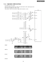
Страница 222: ...ynchronizing for reading 2 Motor operation During motor driving pin 98 of ASIC IC604 becomes a high level motor driver IC51 becomes active mode Stepping pulses are output from ASIC IC604 pins 100 105 causing driver IC51 pins 4 6 7 and 9 to drive the motor coil The motor coil is energized sequentially in 2 phase increments which causes a 1 step rotation A 1 step rotation feeds 0 042mm of document p...

Страница 223: ...223 KX FLB852CX KX FLB852CXS ...

Страница 224: ...7 7 2 2 ADF Auto Document Feed MOTOR DRIVE CIRCUIT 224 KX FLB852CX KX FLB852CXS ...

Страница 225: ...4 Q55 turns ON As a result 5V is supplied to pin 20 and pin 23 of IC52 When the level of these pins become 5V enough current to drive the motor can be supplied from motor driver Stepping pulses are output from ASIC IC604 pins 100 105 causing driver IC52 pins 3 7 8 and 12 to drive the motor coil The motor coil is energized sequentially in 2 phase increments which causes a 1 step rotation A 1 step r...

Страница 226: ...226 KX FLB852CX KX FLB852CXS ...

Страница 227: ...7 7 3 2 FB Flat Bed MOTOR DRIVE CIRCUIT 227 KX FLB852CX KX FLB852CXS ...

Страница 228: ...7 8 DRIVE MODE AND WAVEFORM OF ADF AND FB MOTOR 1 Correspondent table of operation mode and waveform 2 Waveform Figure 1 phase pattern Flat torque 1 2 phase excitation 228 KX FLB852CX KX FLB852CXS ...

Страница 229: ...Figure 2 phase pattern W1 2 phase excitation Figure 3 phase pattern Flat torque 1 2 phase excitation 229 KX FLB852CX KX FLB852CXS ...

Страница 230: ...Figure 4 phase pattern W1 2 phase excitation Figure 5 phase pattern Normal torque 1 2 phase excitation 230 KX FLB852CX KX FLB852CXS ...

Страница 231: ...activated In this case the pulse signal as shown below input to pin P16 of IC600 and the rotation of the FAN is detected 7 9 2 Front Fan Fan2 The signal level at pin 83 84 of IC604 becomes high the FAN is activated In this case the pulse signal as shown below input to pin P18 of IC600 and the rotation of the FAN is detected 231 KX FLB852CX KX FLB852CXS ...

Страница 232: ...rotates at low speed Approx 2200 rpm when the temperature of the unit goes up over a fixed one or depending on the number of printed papers frequency While the fan is rotating at high speed the voltage of Approx 21 V is supplied to the fan however while rotating at low speed the supply voltage is decreased to Approx 12V Each signal wave is as follows 1 High speed rotation typ 3000 rpm 2 Low speed ...

Страница 233: ...ch The solenoid is designed to be driven by 24V Diode protects Transistor from backward voltage when the solenoid is driven REGIST Mode IC600 H1 Solenoid ON High level Solenoid OFF Low level MANUAL Mode IC600 H3 Solenoid ON High level Solenoid OFF Low level PICKUP Mode IC600 R3 Solenoid ON High level Solenoid OFF Low level SORTER 233 KX FLB852CX KX FLB852CXS ...

Страница 234: ...Mode IC600 J3 Solenoid ON High level Solenoid OFF Low level 2nd PICKUP Mode IC600 G1 Solenoid ON High level Solenoid OFF Low level 234 KX FLB852CX KX FLB852CXS ...

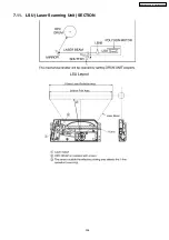
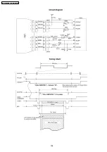
Страница 235: ...7 11 LSU Laser Scanning Unit SECTION 235 KX FLB852CX KX FLB852CXS ...

Страница 236: ...236 KX FLB852CX KX FLB852CXS ...

Страница 237: ...F PAPER INPUT TRAY 2 ADF cover sensor Sensor PCB SW21 CLOSE ADF COVER FB cover sensor Sensor PCB SW23 Top cover sensor H V S P SW1 TOP COVER OPEN Toner sensor Sensor PCB IC40 TONER EMPTY TONER LOW CHECK DRUM Option cassette cover sensor Op cassette PCB SW953 CHECK INSTALL INPUT TRAY 3 Option cassette paper sensor Op cassette PCB SW951 OUT OF PAPER INPUT TRAY 3 Option cassette pickup sensor Op cass...

Страница 238: ... high level Signal IC600 N16pin Paper exist Low level No papers High level 7 12 3 PICKUP SENSOR This Switch detects whether a recording paper is picked up or not When there is a recording paper at the position of the switch the input signal of IC604 96pin becomes low level When there is no recording paper at the position of the switch the input signal of IC604 96pin becomes high level Signal IC604...

Страница 239: ...l of IC604 27pin becomes high level Signal IC604 27pin A paper exists Low level No papers High level 7 12 5 SORTER BIN1 SENSOR This sensor detects whether an output tray 1 is full of paper or not When the output tray is full of paper the input signal of IC604 28pin becomes high level When the output tray is not full of paper the input signal of IC604 28pin becomes low level Signal IC604 28pin TRAY...

Страница 240: ...es low level Signal IC604 29pin TRAY 2 is full High level TRAY 2 is not full Low level 7 12 7 SORTER BIN3 SENSOR This sensor detects whether an output tray 3 is full of paper or not When the output tray is full of paper the input signal of IC604 28pin becomes high level When the output tray is not full of paper the input signal of IC604 28pin becomes low level Signal IC604 30pin TRAY 3 is full Hig...

Страница 241: ...whether the carriage is at it s home position or not When the carriage is at it s home position a shelter plate closes the sensor light So the photo transistor turns off and the input signal of IC604 110pin becomes high level When the carriage is not at it s home position a shelter plate lets the sensor light pass So the photo transistor turns on and the input signal of IC604 110pin becomes low le...

Страница 242: ... Photo transistor Signal IC604 111pin A document exits OFF High level No document ON Low level 7 12 11 REGISTRATION SENSOR This sensor detects whether the recording paper is at the sensor position When the recording paper is detected the shelter plate lets the sensor light pass So the photo transistor turns on and input signal of IC604 112pin becomes low level When the recording paper is not detec...

Страница 243: ...mes high level Photo transistor Signal IC604 113pin Paper exits ON Low level No paper OFF High level 7 12 13 DOCUMENT SENSOR This sensor detects whether a document is set in ADF or not When a document is set in ADF the shelter plate closes the sensor light So the photo transistor turns off and input signal of IC604 115pin becomes high level When a document is not set in ADF the shelter plate lets ...

Страница 244: ...put signal of IC604 116pin becomes high level Photo transistor Signal IC604 116pin Paper exits OFF High level No paper ON Low level 7 12 15 ADF COVER SENSOR This switch detects whether ADF cover is opened or closed When ADF cover is opened the input signal of IC604 117pin becomes high level When ADF cover is closed the input signal of IC604 117pin becomes low level Signal IC604 117pin Cover open H...

Страница 245: ...604 118pin Cover open High level Cover close Low level 7 12 17 TOP COVER SENSOR The Switches detect whether the printer cover is open or closed When the printer cover is closed the switches turn ON and the input signal of IC604 97pin becomes a high level When the printer cover is open the switches turns OFF and the input signal of IC604 97pin becomes a low level Switch Signal IC604 97pin Open OFF ...

Страница 246: ...pendulum of Mixing Paddle The pendulum is pushed up by the Mixing Paddle then it falls down by its own weight The rotation speed of paddle is set slower than the one of pendulum which falls down by its own weight When the toner is still left the pendulum falls and stops on the toner then pushed by the paddle it starts to rotate When no toner is left the pendulum falls to the bottom Consequently th...

Страница 247: ...l at only printing It is not executed at 2 Toner full can be judged by continuous 3 times TONER FULL signal at initialization It is not executed at printing 3 In the ordinal operation CHECK DRUM is displayed when TONER EMPTY sensor does not generate a signal for 2 73 seconds 247 KX FLB852CX KX FLB852CXS ...

Страница 248: ...7 12 18 2 Drum Detection 248 KX FLB852CX KX FLB852CXS ...

Страница 249: ...vel Signal IC600 P17pin Cover open High level Cover close and tray set Low level 7 12 20 OPTION CASSETTE PAPER SENSOR This switch detects whether there are recording papers in the paper tray 3 When there are recording papers in the tray the input signal of IC600 R16pin becomes high level When there are no recording papers in the tray the input signal of IC600 R16pin becomes low level Signal IC600 ...

Страница 250: ...at the position of the switch the input signal of IC604 89pin becomes high level Signal IC604 89pin Paper exist Low level No paper High level 7 12 22 OPTION CASSETTE PAPER TRAY SENSOR This switch detects whether the paper tray 3 is set or not When the paper tray is set and side cover of option cassette is closed the signal of IC600 P17pin becomes low level When the paper tray is not set the signal...

Страница 251: ... the switch is turned off and the signal of IC600 K16pin becomes low level When the option handset is settled the switch is turned on and the signal of IC600 K16pin becomes high level Signal IC600 K16pin ON HOOK High level OFF HOOK Low level 251 KX FLB852CX KX FLB852CXS ...

Страница 252: ...KIN0 KIN1 KIN2 KIN3 KIN4 KIN5 KIN6 KIN7 KSL0 2 1 3 STOP FAX MENU Caller ID KSL1 5 4 6 Sorter Mode HELP Auto Answer KSL2 8 7 9 SET COPY S1 CLEAR S6 KSL3 FLASH REDIAL MONITOR START S2 ZOOM S7 KSL4 0 RESOLUTION SCAN PAPER TRAY CONTRAST S8 LED7 should be set to KSL4 8 x 5 key matrix is executed by hardware scanning b Soft Scan SKIN0 XLED11 KIN1 XLED12 KIN2 XLED13 SKS0 XLED9 S5 S3 SKS1 XLED10 S9 S4 S10...

Страница 253: ... ASCII code from the data bus D4 D7 V0 is supplied for the crystal drive R118 and R117 are density control resistors Consequently in this unit the timing positive clock is generated by the LCD interface circuitry in the gate array IC101 253 KX FLB852CX KX FLB852CXS ...

Страница 254: ...4 35KV 47 5 10V 230V 15V 50 300V PWM20 300V 15Vp p 17 5KHz 100MΩ 1400V 800V 100V Nominal Output Current 200 15µA 200µA 300MΩ 14 8µA 1µA 0µA 25µA PWM 35 1000MΩ 1 25µA Load Range 19 4MΩ 100MΩ 2000MΩ 100MΩ 2000MΩ 33 8MΩ 284MΩ 10MΩ 1000MΩ Constant Current Range 4 1 4 6KV 4200V 500V As for the developing voltage the DC voltage and AC voltage are overlapped and output from an output terminal There is on...

Страница 255: ...rature 7 15 4 DEV AC BIAS UNIT When 17 5kHz rectangular wave signal is input from IC600 to DEV AC through transistor Q639 325 Vp p 17 5 kHz rectangular wave of developing AC voltage is output from DEV OUTPUT This voltage is overlapped with developing DC voltage and output as AC voltage that includes the development DC voltage 7 15 5 TRA BIAS Transfer BIAS TRA BIAS Transfer BIAS UNIT When CHG REM i...

Страница 256: ...the heater control port IC604 41pin and is turned ON OFF at the triac SCR101 And two thermostats are set on the AC line as the safety devices 1 Control at Printing a After the printing signal is received turn ON the heater b After that turn ON the motor at the Primary Stable Temperature 170 C c After that control at the Secondary Stable temperature 205 C and feed papers 256 KX FLB852CX KX FLB852CX...

Страница 257: ...2 Safety Protection a 2 thermostats are provided with the unit and the heater circuit is shut down when their surface temperatures became over 257 KX FLB852CX KX FLB852CXS ...

Страница 258: ... C4 173 88 58 6 251 FB 90 195 C3 174 87 57 7 250 FA 91 193 C1 175 86 56 8 250 FA 92 192 C0 176 85 55 9 250 FA 93 191 BF 177 84 54 10 250 FA 94 190 BE 178 83 53 11 249 F9 95 188 BC 179 82 52 12 249 F9 96 187 BB 180 81 51 13 249 F9 97 186 BA 181 80 50 14 249 F9 98 184 B8 182 79 4F 15 248 F8 99 183 B7 183 78 4E 16 248 F8 100 182 B6 184 77 4D 17 248 F8 101 181 B5 185 76 4C 18 248 F8 102 179 B3 186 75 ...

Страница 259: ...5 139 129 81 223 48 30 56 228 E4 140 127 7F 224 48 30 57 228 E4 141 126 7E 225 47 2F 58 227 E3 142 125 7D 226 46 2E 59 226 E2 143 123 7B 227 46 2E 60 225 E1 144 122 7A 228 45 2D 61 224 E0 145 121 79 229 45 2D 62 224 E0 146 120 78 230 44 2C 63 223 DF 147 118 76 231 44 2C 64 222 DE 148 117 75 232 43 2B 65 221 DD 149 116 74 233 43 2B 66 220 DC 150 114 72 234 42 2A 67 219 DB 151 113 71 235 42 2A 68 21...

Страница 260: ...8 12 6 171 AB 41 60 3C 88 17 11 5 168 A8 42 58 3A 89 17 11 4 166 A6 43 57 39 90 16 10 3 163 A3 44 55 37 91 16 10 2 160 A0 45 54 36 92 16 10 1 158 9E 46 52 34 93 15 0F 0 155 9B 47 51 33 94 15 0F 1 152 98 48 50 32 95 14 0E 2 150 96 49 48 30 96 14 0E 3 147 93 50 47 2F 97 14 0E 4 144 90 51 46 2E 98 13 0D 5 141 8D 52 45 2D 99 13 0D 6 139 8B 53 43 2B 100 13 0D 7 136 88 54 42 2A 101 12 0C 8 133 85 55 41 ...

Страница 261: ...C AD value HEX reading Temperature C AD value HEX reading 21 100 64 68 29 1D 115 9 09 22 97 61 69 28 1C 116 9 09 23 95 5F 70 27 1B 117 8 08 24 93 5D 71 27 1B 118 8 08 25 91 5B 72 26 1A 119 8 08 26 88 58 73 25 19 120 8 08 261 KX FLB852CX KX FLB852CXS ...

Страница 262: ... L Over voltage Q1 A B Voltage Wave Form C D Voltage Wave Form E F G H Voltage Wave Form 0 0 0 T1 PC1 Triac SCR1 Heat Lamp Photo Triac Coupler PC2 Block Diagram 3 3V Output Circuit Input Circuit The input current goes into the input rectifier circuit through the filter circuit The filter circuit decreases the noise voltage and the noise electric field strength Rectifier Circuit The input circuit i...

Страница 263: ...Load L Then the power is supplied to the Load When Q1 is ON power is not output from the secondary side The output voltage is fed back in the control IC according to the error amp rectifier Then depending on how TON is controlled stabilization occurs Also when the current load becomes too large in order to decrease the voltage output the increase in is controlled and the output voltage is stabiliz...

Страница 264: ...pler PC1 increases the pulse width of the output control IC becomes narrower and the ON period of Q1 becomes shorter Over Current Limiter O C L The highest drain current of Q1 is limited by a limit current function of IC1 The 24V output is limited by this function Over Voltage Circuit If the 24V output increases because the error detecting circuit or control circuit is broken IC1 will recognize th...

Страница 265: ...ed electric potential The sensitive drum is the Organic Photo Conductor OPC which is a electric conductive cylinder whose surface is covered with the Charge Generation Transfer Layer CGTL When the charging bias DC 4 35kv is added and the plus charge is supplied to the opc surface while charging the whole surface potential of the drum is 475V Charging Part 265 KX FLB852CX KX FLB852CXS ...

Страница 266: ...er Layer which conducts the minus charge the plus charged drum s surface is neutralized to be skipped Then the plus charge goes to the ground from the electric conductive cylinder Consequently the charge of the part which is not exposed remains as it is and the electric potential of the scanned part changes At that time an invisible image is created on the drum Exposing Part 8 1 4 LASER SCANNING U...

Страница 267: ...ce causes to send the toner to the developing roller from the toner supply roller The supplied toner to the developing roller is kept to a certain layer thickness by the developing blade and also it is charged by triboelectricity Consequently the toner is transferred to the surface of the exposed OPC drum by the potential difference between the developing roller and OPC drum s surface The transfer...

Страница 268: ... stage that cleans the remain toner after the transcription stage The remain toner on the drum and the toner which was attached to the place where the laser beam didn t scan are gathered to the developing roller to be used again After paper jam or replacing toner and drum unit the transfer roller is plus charged to eliminate the plus charged toner Cleaning Part 268 KX FLB852CX KX FLB852CXS ...

Страница 269: ...t from attaching the toners The press roller is made of silicon and its spring compresses the melted toner Fixing Part The fixing part becomes high temperature so the thermistor and the thermal fuse are provided 1 Thermistor The thermistor touches the heat roller and check the temperature to feed back to the control circuit The surface temperature should be kept 205 C while printing 2 Thermostat T...

Страница 270: ...8 2 TERMINAL GUIDE OF THE ICs TRANSISTORS AND DIODES 8 2 1 DIGITAL BOARD 8 2 2 ANALOG BOARD 270 KX FLB852CX KX FLB852CXS ...

Страница 271: ...8 2 3 OPERATION BOARD 8 2 4 AFE BOARD 8 2 5 LAN BOARD 8 2 6 CASSETTE RELAY BOARD 271 KX FLB852CX KX FLB852CXS ...

Страница 272: ...8 2 7 HIGH VOLTAGE POWER SUPPLY BOARD 272 KX FLB852CX KX FLB852CXS ...

Страница 273: ...8 2 8 LOW VOLTAGE POWER SUPPLY BOARD 273 KX FLB852CX KX FLB852CXS ...

Страница 274: ...mporarily soldering two diagonally opposite pins in the correct positions on the PCB Be certain each pin is located over the correct pad on the PCB 2 Apply flux to all of the pins on the IC 3 Being careful to not unsolder the tack points slide the soldering iron along the tips of the pins while feeding enough solder to the tip so that it flows under the pins as they are heated 8 3 3 REMOVING SOLDE...

Страница 275: ...and any malfunctions are analyzed In past experiences digital IC especially DRAM and ROM malfunctions are extremely rare after installation in the product This may be repaired by replacing the IC DRAM etc However the real cause may not have been an IC malfunction but a soldering fault instead Soldering faults difficult to detect with the naked eye are common particularly for ASIC and RA Resistor A...

Страница 276: ...8 4 1 NG EXAMPLE 276 KX FLB852CX KX FLB852CXS ...

Страница 277: ... Determined in 1968 Transmission for about 6 minutes at a scanning line density of 3 85 lines mm Group II G2 Using reduction technology in the modulation demodulation format an A 4 size document is sent at an official scanning line density of 3 85 lines mm for about 3 minutes Methods to suppress redundancy are not used Determined in 1976 Group III G3 Method of suppressing redundancy in the image s...

Страница 278: ...ocument was actually sent and to check for telephone reservations and or the existence of continuous transmission 5 Facsimile Standards Item Telephone Network Facsimile G3 Machine Connection Control Mode Telephone Network Signal Mode Terminal Control Mode T 30 Binary Facsimile Signal Format Digital Modulation Mode PSK V 27 ter or QAM V 29 Transmission Speed 300 bps Control Signal 2400 4800 7200 96...

Страница 279: ... Digital Command Signal Identification Signal Format X1000001 Example Some models do not support the following items Bit No DIS DTC DCS 1 Transmitter T 2 operation 2 Receiver T 2 operation Receiver T 2 operation 3 T 2 IOC 176 T 2 IOC 176 4 Transmitter T 3 operation 5 Receiver T 3 operation Receiver T 3 operation 6 Reserved for future T 3 operation features 7 Reserved for future T 3 operation featu...

Страница 280: ...0 0 0 0 0 1 0 1 0 1 0 0 0 1 1 1 1 0 1 0 1 1 1 1 Minimum scan line time capability of the receiver 20 ms at 3 85 l mm T7 7 T3 85 40 ms at 3 85 l mm T7 7 T3 85 10 ms at 3 85 l mm T7 7 T3 85 5 ms at 3 85 l mm T7 7 T3 85 10 ms at 3 85 l mm T7 7 1 2 T3 85 20 ms at 3 85 l mm T7 7 1 2 T3 85 40 ms at 3 85 l mm T7 7 1 2 T3 85 0 ms at 3 85 l mm T7 7 T3 85 Minimum scan line time 20 ms 40 ms 10 ms 5 ms 0 ms 2...

Страница 281: ...nfirmation to Receive X0100001 Notifies the sending side that TCF has been properly received If TCF is not properly received FTT Failure To Train X0100010 is relayed to the sender The sender then reduces the transmission speed by one stage and initiates training once again Training 2 Used for reconfirming the receiving side like training 1 Image Signal Refer to the next page RTC Return to Control ...

Страница 282: ...282 KX FLB852CX KX FLB852CXS ...

Страница 283: ...8 6 TEST CHART 8 6 1 ITU T No 1 TEST CHART 283 KX FLB852CX KX FLB852CXS ...

Страница 284: ...8 6 2 ITU T No 2 TEST CHART 284 KX FLB852CX KX FLB852CXS ...

Страница 285: ...9 FIXTURES AND TOOLS 285 KX FLB852CX KX FLB852CXS ...

Страница 286: ...10 CABINET MECHANICAL AND ELECTRICAL PARTS LOCATION 10 1 OPERATION PANEL SECTION 286 KX FLB852CX KX FLB852CXS ...

Страница 287: ...10 2 PRINTER COVER SECTION 1 287 KX FLB852CX KX FLB852CXS ...

Страница 288: ...10 3 PRINTER COVER SECTION 2 288 KX FLB852CX KX FLB852CXS ...

Страница 289: ...10 4 ADF SECTION 289 KX FLB852CX KX FLB852CXS ...

Страница 290: ...10 5 PRINTER COVER SECTION 3 290 KX FLB852CX KX FLB852CXS ...

Страница 291: ...10 6 MANUAL TRAY SECTION 291 KX FLB852CX KX FLB852CXS ...

Страница 292: ...10 7 MULTI ROLLER SECTION 292 KX FLB852CX KX FLB852CXS ...

Страница 293: ...10 8 UPPER MAIN CABINET SECTION 293 KX FLB852CX KX FLB852CXS ...

Страница 294: ...10 9 FUSER SECTION 294 KX FLB852CX KX FLB852CXS ...

Страница 295: ...10 10 REAR COVER SECTION 295 KX FLB852CX KX FLB852CXS ...

Страница 296: ...10 11 MOTOR SECTION 296 KX FLB852CX KX FLB852CXS ...

Страница 297: ...10 12 GEAR CHASSIS SECTION 297 KX FLB852CX KX FLB852CXS ...

Страница 298: ...10 13 LOWER MAIN CABINET SECTION 298 KX FLB852CX KX FLB852CXS ...

Страница 299: ...10 14 SORTER FRAME AND DOCUMENT TRAY SECTION 299 KX FLB852CX KX FLB852CXS ...

Страница 300: ...10 15 CASSETTE SECTION 300 KX FLB852CX KX FLB852CXS ...

Страница 301: ...10 16 SORTER SIDE SECTION 301 KX FLB852CX KX FLB852CXS ...

Страница 302: ...10 17 SCREW AND LEAD WIRE LAYOUT OF SORTER 302 KX FLB852CX KX FLB852CXS ...

Страница 303: ...10 18 SORTER MAIN SECTION 303 KX FLB852CX KX FLB852CXS ...

Страница 304: ...10 19 SORTER TOP SECTION 304 KX FLB852CX KX FLB852CXS ...

Страница 305: ...10 20 HANDSET CRADLE SECTION 305 KX FLB852CX KX FLB852CXS ...

Страница 306: ...10 21 KX FA101E KX FA101A PAPER CASSETTE SECTION OPTION 306 KX FLB852CX KX FLB852CXS ...

Страница 307: ...10 21 1 FRAME SECTION 1 307 KX FLB852CX KX FLB852CXS ...

Страница 308: ...10 21 2 FRAME SECTION 2 308 KX FLB852CX KX FLB852CXS ...

Страница 309: ...10 21 3 LOWER CASSETTE SECTION 309 KX FLB852CX KX FLB852CXS ...

Страница 310: ...10 22 KX FA102E LAN BOARD OPTION 310 KX FLB852CX KX FLB852CXS ...

Страница 311: ...10 23 ACTUAL SIZE OF SCREWS AND WASHER 311 KX FLB852CX KX FLB852CXS ...

Страница 312: ...11 ACCESSORIES AND PACKING MATERIALS 312 KX FLB852CX KX FLB852CXS ...

Страница 313: ...020Z1 COVER ABS HB 13 PFBX1243Z2 PUSH BUTTON FCS ABS HB 14 PFBX1242Z2 PUSH BUTTON FUNCTION ABS HB 15 PFBX1241Z2 PUSH BUTTON STATION ABS HB 16 PFBC1143Z2 PUSH BUTTON NAVIGATOR ABS HB 17 PFGE1019Z1 COVER ABS HB 12 1 2 PRINTER COVER SECTION 1 Ref No Part No Part Name Description Remarks 30 PFQT2488Z LABEL LIFT TO OPEN 31 PFHX1897X SPACER 32 PFHX1887X CASE COVER 33 N2GADE000001 PHOTO ELECTRIC TRANSDUC...

Страница 314: ...AR POM HB 172 PFDJ1083Y SPACER 173 PFDN1076Y ROLLER 174 PFDJ1083Z SPACER POM HB 175 PFUE1024X FRAME PS HB 176 PFNPB031054 WASHER Ref No Part No Part Name Description Remarks 177 PFHX1937Z SHEET ADF EARTH 12 1 5 PRINTER COVER SECTION 3 Ref No Part No Part Name Description Remarks 190 PFHE1178Z SPACER 191 PFHR1475Z GUIDE 192 PFMH1159Z METAL PARTS 193 PFDJ1042Z SPACER POM HB 194 PFDS1019Z ROLLER 195 ...

Страница 315: ... ROLLER POM HB 348 PFDF1098Z SHAFT 349 PFUS1601Z COIL SPRING 350 PFDJ1085Z SPACER 351 PFDN1079Z ROLLER 352 PFDJ1085Y SPACER POM HB Ref No Part No Part Name Description Remarks 353 PFDG1419Z GEAR POM HB 354 PFDE1251Z SPACER POM HB 355 PFUS1684Z COIL SPRING 356 PFKM1166Y1 CABINET BODY PS 5V 357 PFQT2490Y LABEL 358 PFJV1009Z DUCT BRUSH DISCHARGE 359 PFHX1937Z SHEET ADF EARTH 360 PFSE1025Z SHEET DUCT ...

Страница 316: ...BBER PARTS 516 PFMD1086W CHASSIS 517 PFJS03N22Z CONNECTOR Ref No Part No Part Name Description Remarks 518 WLL20YG27M3M LEAD WIRE 519 PFUS1639Z COIL SPRING 520 PFUS1593Y COIL SPRING 521 PFUS1028Z LEAF SPRING 522 PF0M1005Z MIRROR 523 PFUS1597Z COIL SPRING 524 PFUS1451Z COIL SPRING 525 PFUE1034Y LEVER PS HB 526 PFUE1035Y CHASSIS PS 5V 527 PFUS1576Z LEAF SPRING 528 PFUS1599Y BAR SPRING 529 PFUS1577Z ...

Страница 317: ...142P314 SPRING 766 PF4142P025 ROLLER 767 PF4142P043 GUIDE 768 PF4142P312 ROLLER 769 PF4142P028 ROLLER Ref No Part No Part Name Description Remarks 770 PF4142P027 GEAR 771 PF4142P009 CHASSIS 772 PF4142P044 SPACER 773 PF4142P084 GEAR 774 PF4142P010 CHASSIS 775 PF4142P310 BRUSH 776 PF4142P023 LEVER 777 PF4142P024 LEVER 778 PF4142P001 FRAME 12 1 18 SORTER TOP SECTION Ref No Part No Part Name Descripti...

Страница 318: ...1010 PFPK2918Z M PACKING CASE KX FA101A 1011 PFHG1259Z SPACER 12 1 23 KX FA102E KX FA102A LAN BOARD OPTION Ref No Part No Part Name Description Remarks 1015 PFHX1880Y SPACER 1016 PFMH1176Y FRAME 1017 PFKV1114Y1 COVER 1018 Not used 1019 XZB05X08Z03 PLASTIC BAG 1020 PFQT2510Z LABEL MAC Addr 1021 PFGT2842Z M NAME PLATE KX FA102E 1021 PFGT2841Z M NAME PLATE KX FA102A 1022 PFPP1031Z PROTECTION COVER 10...

Страница 319: ... 33p C578 ECUV1H330JCV 33p C579 ECUV1H101JCV 100p C580 ECUV1H330JCV 33p C581 ECUV1H330JCV 33p C582 ECUV1H330JCV 33p C583 ECUV1H330JCV 33p C584 ECUV1H101JCV 100p C591 ECUV1H330JCV 33p C603 ECUV1H150JCV 15p C604 ECUV1H150JCV 15p C605 ECUV1C104ZFV 0 1 Ref No Part No Part Name Description Remarks C606 ECUV1H103KBV 0 01 C607 ECUV1H103KBV 0 01 C608 ECUV1C104ZFV 0 1 C609 ECUV1C104ZFV 0 1 C610 ECUV1C104ZF...

Страница 320: ...760 ECEA1CKA100 10 C761 ECUV1H102KBV 0 001 C762 ECUV1C104ZFV 0 1 C763 ECUV1C104ZFV 0 1 Ref No Part No Part Name Description Remarks C764 ECUV1C104ZFV 0 1 C765 ECUV1C104ZFV 0 1 C766 ECUV1C104ZFV 0 1 C767 ECUV1C104ZFV 0 1 C768 ECUV1C104ZFV 0 1 C769 ECUV1C104ZFV 0 1 C770 ECUV1C104ZFV 0 1 C771 ECUV1C104ZFV 0 1 C772 ECUV1C104ZFV 0 1 C773 ECUV1C104ZFV 0 1 C774 ECUV1C104ZFV 0 1 C775 ECUV1C104ZFV 0 1 C776...

Страница 321: ... Name Description Remarks L569 PFVF1B601ST CERAMIC FILTER S L602 PFVF1B601ST CERAMIC FILTER S L603 PFVF1B601ST CERAMIC FILTER S L604 PFVF1B601ST CERAMIC FILTER S L605 PFVF1B601ST CERAMIC FILTER S L606 PFVF1B601ST CERAMIC FILTER S L607 PFVF1B601ST CERAMIC FILTER S L608 PFVF1B601ST CERAMIC FILTER S L609 PFVF1B601ST CERAMIC FILTER S L610 PFVF1B252SDT CERAMIC FILTER S L615 PFVF1B601ST CERAMIC FILTER S...

Страница 322: ...627 ERJ3GEYJ563 56k R628 ERJ12YJ471 470 R629 ERJ12YJ390 39 R630 ERJ12YJ471 470 R631 ERJ3GEYJ103 10k R632 ERJ3GEYJ103 10k R633 PQ4R10XJ822 8 2k S R634 PQ4R10XJ822 8 2k S R635 ERJ3GEYJ330 33 R636 ERJ3GEYJ473 47k R637 PQ4R10XJ822 8 2k S R638 PQ4R10XJ822 8 2k S Ref No Part No Part Name Description Remarks R639 ERJ3GEYJ103 10k R640 ERJ3GEYJ103 10k R641 ERJ12YJ471 470 R642 ERJ12YJ390 39 R643 ERJ12YJ471 ...

Страница 323: ...V RESISTOR ARRAY RA601 EXB38V473JV RESISTOR ARRAY RA602 D1H83304A010 RESISTOR ARRAY S RA603 D1H83304A010 RESISTOR ARRAY S RA604 D1H83304A010 RESISTOR ARRAY S RA605 EXB28V470JX RESISTOR ARRAY RA606 EXB28V470JX RESISTOR ARRAY RA607 EXRV8V470JV RESISTOR ARRAY S RA608 EXRV8V470JV RESISTOR ARRAY S RA609 EXB28V470JX RESISTOR ARRAY RA610 EXB28V470JX RESISTOR ARRAY RA611 D1H83304A010 RESISTOR ARRAY S RA61...

Страница 324: ...303 ECUV1C104KBV 0 1 C305 ECUV1H820JCV 82p C306 ECUV1H820JCV 82p C307 ECUV1H820JCV 82p C308 ECJ1VC1H680J 68p C309 ECKD2H681KB 680p S C310 ECKD2H681KB 680p S C311 F0C2E105A146 S C313 ECJ1VC1H681J 680p C314 ECUV1H104KBV 0 1 C315 ECUV1H103KBV 0 01 C316 ECUV1H101JCV 100p C317 F2A1C1000030 C319 ECUV1H103KBV 0 01 C321 ECEA1CK470 47 S C322 ECUV1H103KBV 0 01 C325 ERJ3GEY0R00 0 C329 ECUV1C104ZFV 0 1 C330 F...

Страница 325: ...J3GEYJ103 10k R266 ERJ3GEYJ104 100k R267 ERJ3GEYJ562 5 6k R269 ERJ3GEYJ104 100k R270 ERJ3GEYJ821 820 R271 ERJ3GEYJ223 22k Ref No Part No Part Name Description Remarks R272 ERJ3GEYJ243 24k R273 ERDS2TJ150 15 S R274 ERJ3GEYJ102 1k R275 ERJ3GEYJ101 100 R276 ERJ3GEYJ392 3 9k R279 ERJ3GEYJ154 150k R280 ERJ3GEYJ124 120k R282 ERJ3GEYJ153 15k R283 ERJ3GEYJ103 10k R285 PQ4R18XJ100 10 S R286 ERJ3GEYJ303 30k...

Страница 326: ...J181 180 Ref No Part No Part Name Description Remarks R105 ERJ3GEYJ391 390 R106 ERJ3GEYJ391 390 R107 ERJ3GEYJ241 240 R109 ERJ3GEYJ181 180 R110 ERJ3GEYJ181 180 R111 ERJ3GEYJ181 180 R112 ERJ3GEYJ181 180 R113 ERJ3GEYJ241 240 R114 ERJ3GEYJ241 240 R116 ERJ3GEYJ123 12k R117 ERJ3GEYJ333 33k R118 ERJ3GEYJ912 9 1k R119 ERJ3GEYJ4R7 4 7 R121 ERJ3GEYJ561 560 R122 ERJ3GEYJ101 100 R123 ERJ3GEYJ101 100 R124 ERJ3...

Страница 327: ...JCV 33p C98 ECUV1C334ZFV 0 33 C99 ECUV1H330JCV 33p C187 F2G0J1010014 100 C188 ECUV1H390JCV 39p Ref No Part No Part Name Description Remarks C189 ECUV1H390JCV 39p C190 ECUV1H390JCV 39p C191 ECUV1H103KBV 0 01 C192 ECUV1H101JCV 100p C193 ECUV1H102KBV 0 001 C194 ECUV1H102KBV 0 001 C196 ECUV1H101JCV 100p C197 ECUV1H330JCV 33p C198 ECUV1H330JCV 33p C199 ECUV1H330JCV 33p FILTERS FLT51 J0MAB0000006 IC FIL...

Страница 328: ... S Ref No Part No Part Name Description Remarks D2 1SS133 DIODE SI S D3 1SS133 DIODE SI S CONNECTORS CN2 K1KA02AA0193 CONNECTOR 2P CN3 K1KA03AA0193 CONNECTOR 3P CN4 K1KA02AA0224 CONNECTOR 2P CN5 K1KA02AA0193 CONNECTOR 2P CN6 K1KA07A00257 CONNECTOR 7P CAPACITOR C4 ECEA1VKA101 100 S 12 16 VARISTOR BOARD PARTS Ref No Part No Part Name Description Remarks PCB14 PFLP1694MZ J VARISTOR BOARD ASS Y RTL VA...

Страница 329: ...0k R41 ERJ3GEYF333 33k R42 ERJ3GEYJ563 56k R43 ERJ3GEYJ222 2 2k R44 ERJ3GEYJ225 2 2M R45 ERJ3GEYJ225 2 2M Ref No Part No Part Name Description Remarks R46 ERJ3GEYJ225 2 2M R47 ERJ3GEYJ225 2 2M R48 ERJ6GEYJ106 10M R49 ERJ6GEYJ106 10M R50 ERJ3GEYJ102 1k R54 ERJ3GEYF434 430k R55 ERJ3GEYJ225 2 2M R58 ERJ3GEYF243 24k R64 ERJ3GEYJ472 4 7k R65 ERJ3GEYF184 180k R66 ERJ3GEYJ103 10k R67 ERJ3GEYF274 270k R68...

Страница 330: ...R00 0 J109 ERJ6GEY0R00 0 J111 ERJ6GEY0R00 0 R1 PFRDT26A105 1M S R2 PQ4R10XJ103 10k S R3 PQ4R10XJ103 10k S R4 ERDS2TJ103 10k Ref No Part No Part Name Description Remarks R5 PQ4R10XJ103 10k S R6 PQ4R10XJ101 100 S R7 ERJ6GEYJ100 10 R8 ERJ6GEY0R00 0 R9 ERDS2TJ101 100 S R10 ERJ6GEYF472V 4 7k R19 ERJ3GEYJ122 1 2k R20 ERDS2TJ101 100 S R21 ERDS2TJ101 100 S R22 PFRDT26A100 10 S R23 ERJ6GEYJ151 150 R30 ERX2...

Страница 331: ...3GEYJ103 10k R924 ERJ3GEYJ103 10k R927 ERJ3GEYJ103 10k R928 PQ4R10XJ331 330 S CRYSTAL RESONATOR X900 H0J250500055 CRYSTAL RESONATOR 12 21 HOOK SWITCH BOARD OPTION Ref No Part No Part Name Description Remarks PCB19 PFLP1696MZ HOOK SWITCH BOARD RTL JACKS CN940 PQJJ1TC5Z JACK S CN941 K2LA104B0019 JACK SWITCH SW940 ESE14A211 SWITCH 12 22 CASSETTE RELAY BOARD PARTS OPTION Ref No Part No Part Name Descr...

Страница 332: ...Z3K5Z EXTENSION CORD 3P EC2 PFZZ30K1Z EXTENSION CORD 30P EC3 PQZZ3K12Z EXTENSION CORD 3P EC4 PFZZ7K18ZA EXTENSION CORD 7P EC5 PQZZ7K5Z EXTENSION CORD 7P EC6 PQZZ5K6Z EXTENSION CORD 5P EC7 PFZZ8K4ZZ EXTENSION CORD 8P EC8 PQZZ2K1Z EXTENSION CORD 2P EC9 PFZZ8K18Z EXTENSION CORD 8P EC10 PFZZ13K3Z EXTENSION CORD 13P EC11 PFZZ11K13Z EXTENSION CORD 13P EC12 PFZZ30K2Z EXTENSION CORD 30P EC13 PQZZ22K2Z EXT...

Страница 333: ...S Note 1 DC voltage measurements are taken with an oscilloscope or a tester with a ground 2 The schematic diagrams and circuit board may be modified at any time with the development of new technology 3 333 KX FLB852CX KX FLB852CXS ...

Страница 334: ...MEMO 334 KX FLB852CX KX FLB852CXS ...

Страница 335: ...D 4 J2 SD 5 V2 SD 6 K1 SD 7 T3 SSEN T6 CCDCLK 0 U6 CCDCLK 1 V6 CCDCLK 2 T5 CCDCLK 3 U5 CCDCLK 4 V5 CCDILL 0 T4 CCDILL 1 U4 CCDILL 2 A13 SPICLK B12 SPIDO A12 SPIDI G3 SMOT 0 G2 SMOT 1 G1 SMOT 2 J3 SMOT 3 H3 SMOT 4 H1 SMOT 5 R3 SMOT 6 C15 GPIO 0 B15 GPIO 1 A15 GPIO 2 C14 GPIO 3 B14 GPIO 4 A14 GPIO 5 C13 GPIO 6 B13 GPIO 7 A17 RXD GPIO 34 A16 TXD GPIO 35 B16 RTS GPIO 36 C16 CTS GPIO 37 IC600 SOC N15 V...

Страница 336: ...CG 26 CG 27 3 3V 28 5V 29 12V 30 12V L689 1P181 L688 1P181 L687 1P181 C813 Z0 1u C814 Z0 1u CN604 1 2 DET 3 FANON L629 NC 1 2 3 4 L621 1B601 L620 1B601 L628 1B601 L616 1B601 L619 1B601 L627 1B601 L615 1B601 Q603 Q605 Q606 Q604 CN601 1 VBU S 2 D 3 D 4 GND 470 1 2W R641 470 1 2W R643 470 1 2W R630 470 1 2W R628 IC612 1 2 3 GND 4 5 VCC 3 3V 3 3V IC613 1 2 3 GND 4 5 VCC 3 3V IC614 1 2 3 GND 4 5 VCC IC...

Страница 337: ...76 24V Q616 C678 6 3V100u Z0 1u C802 Z0 1u C803 C671 J18p L680 L681 L682 CN608 1 5V 2 DG 3 M0 4 CR_LED 5 M1 6 CRG 7 M2 8 9 M3 10 PSTART 11 M4 12 FBCVR 13 M5 14 RPS 15 M6 16 ADFCVR 17 PG 18 DOCU 19 24V 20 DOCU_LED 21 ADFENB 22 CRENB J180p C812 J180p C811 X601 32 768KHz 2 2 1 2W R789 2 2 1 2W R790 L636 1B252 L637 1B252 L640 1B252 L639 1B252 L635 1B252 L638 1B252 L634 1B252 L686 1B252 L685 1B252 BAT6...

Страница 338: ...737 3 3K R738 3 3K R740 3 3K Q623 10K R696 Q628 F609 3 15A L672 1P181 4 7K R718 1K R726 3 3V R739 2 2K R741 2 2K OPTPICK 2C X602 22MHz X603 25MHz R698 0 C683 K1u BREAK1 3 5C Z0 1u C805 L657 1B601 L658 1B601 L656 1B601 L668 1B252 L667 1B252 L663 1B252 L665 1B252 L664 1B252 L666 1B252 L661 1B252 L660 1B252 L662 1B252 L659 1B252 L655 K0 1u C693 R717 R715 D604 D605 Q625 Q626 Q622 Q633 R814 100 3 3V C8...

Страница 339: ...K R750 100 C750 Z0 1u C723 J33p RA629 100 1 2 3 4 5 6 7 8 C737 Z0 1u C732 Z0 1u C739 Z0 1u C742 Z0 1u 3 3V R755 10K C748 Z0 1u RA630 100 1 2 3 4 5 6 7 8 3 3V 6 3V330u C727 C729 Z0 1u C753 K1000p 3 3V C741 Z0 1u R760 100 3 3V D 15 0 A 13 0 XMDMRST1 1 2D WR RD XMDMCS1 XMDMINT1 1 5C MICLK MIDAT MILAT LINERLY1 P SHORT1 CIDRLY EVOL0 EVOL1 EVOL2 EXHOOK HOOK DCN1 HSALC1 PICK PAPER DRUM BELL1 TONE BREAK1 ...

Страница 340: ...NC R265 10K K0 027u C256 R244 1K L281 NC R216 110K K6800p C267 C262 J100p 12VA C269 16V10u C247 6 3V330u AG1 L224 1B252 R223 110K L237 1B252 L225 1B252 IC205 1 VCC 2 DET 3 INPUT 4 GND 5 OUTPUT 1B252 L238 R234 J R270 820 L229 1B252 K3900p C259 L223 1B252 L227 1B252 L286 NC C254 K6800p C239 K0 1u L226 1B252 100K R359 C335 NC C241 J68p AG5 AG1 J J202 10K R252 16V10u C330 R229 47K R375 NC D200 Q202 AG...

Страница 341: ... MODEMTXIN 25 MODEMTXOUT 26 NC26 27 TONEIN 28 NC28 29 NC29 30 GND 31 MODEMRXOUT 32 VLIN 33 VREF 34 VLOUT 35 SPOU T 36 SPIN R343 0 5W 6 8 Q210 D205 R335 8 2K 2 2K R302 1K R299 J223 NC F200 24V R329 1K L255 1B252 PC202 A K E C CN204 1 SP 2 SP 10K R295 R306 330K R322 0 5W 47K L245 1B252 L254 1B252 R323 NC R376 NC 10 R285 D207 470K R318 Q216 VREF PC205 A K E C C309 680p 5VD AG4 C299 16V10u C303 K0 1u ...

Страница 342: ... 1H SSP 2H SSP 3A G CN41 1H SMIC 2 HOOK_I N 3H SMIC CN42 1 HSMIC 2 HOOK_IN 3 HSMIC 4 AG 5 HSSP 6 HSSP TO ANALOG BOARD KX FLB852 HANDSET BOARD TO OPTION HANDSET KX FLB852 SENSOR BOARD IC40 1 VCC 2 GND 3 OUTPUT C42 Z0 1u CN43 15 V 2 TNR 3G ND To DIGITAL KX FLB852CX KX FLB852CXS 342 ...

Страница 343: ...0 1u C106 NC S3 SW122 S5 SW128 S4 SW116 C109 J100p C113 K0 01u C120 J100p C119 J100p C121 J100p S6 SW129 SORTOR MODE SW108 SW126 PAPER TRAY SW125 S2 SW124 6 SW120 MONITO R SW118 SW119 ZOOM SW112 STO P SW109 3 SW115 MENU 3 SW121 UTION 2 CALLER ID SW133 COPY SW105 S7 SW130 CLEAR SW111 S8 SW131 9 SW117 AUTO ANSWER SW132 S1 SW123 C107 Z0 1u 5VD C122 6 3V100u 12K R116 12K R127 C116 Z0 1u NC R115 TH101 ...

Страница 344: ...0p R91 100 0 033u R55 C82 C84 1000p C85 22u 4700p C86 D85 R50 1K 10M 10M 430K 24K 2 2K R48 R49 R43 C83 R82 D77 C84 D66 D67 D63 C61 0 068u R70 10K R54 R58 D31 R92 15K R94 4 7K R81 R82 R83 C3 C11 1u 0 1u 0 01u 0 22u 0 1u D1 D2 5 J3 J4 blue 6 7 Grid 3 2 11 IC1 1 4 D81 R89 R87 2 2K Q83 R37 R35 R36 R40 680K C32 R90 33K 33K 100K 220K IC1 Q81 R96 Q84 Q85 Q87 D83 D84 R93 100K Q32 R42 56K B61 Q62 R74 R72 R...

Страница 345: ...7u 0 1u C3X C2 D11 C10 L13 D277 C277 R250 R276 R301 47K 4 7K 10K 10K 0 1u 470 R302 C272 R279 D13 R50 D50 C50 1000p 47K L 1 2 N Q271 C275 Q272 R280 1K Q274 Q301 C D VH NC Vcc Vout CS FB Is GND 1 2 3 4 5 6 7 8 9 10 11 12 12 13 0 1u 0 1u 0 1u 10µsec div 5V div 10µsec div 1V div 10µsec div 0 5V div 10µsec div 10V div 5msec div 20V div Max 166 667V Min 139 583V Max 20 0000V Min 2 29167V 18 40V Max 4 33...

Страница 346: ...K 1K 1K 4 7K 100 R293 D291 IC201 C271 470u 18K D271 C274 1u R278 R277 R303 10K 1K 8 2K 8 2K 2 2K D274 R281 R282 R291 D275 C303 C304 C503 D104 R101 1K R102 R105 R501 330 15K 560 R502 VR101 PC1 R130 PC2 R23 R20 R21 100 150 0 01u 100 DG DG Q292 Q291 C273 0 1u 47K R275 R201 1 1 1 1 1 R202 R203 R204 R205 Q277 R206 4 7K L271 Q275 3 C17 C7 3300p 470p C18 FG 1 2 3 4 5 6 7 8 9 10 11 12 12 13 0 1u 10µsec di...

Страница 347: ... 18 GND18 19 STB 20 CR1 21 VREF1 22 VS1 23 I11 24 I01 25 GND25 26 GND26 Q51 R57 0 3216 2 2K R83 4 7K R84 CN52 1 2 3 4 5 6 7 8 9 10 I 11 12 13 14 15 16 17 18 19 20 21 22 23 24 25 26 27 28 29 30 CN51 1 2 3 4 5 6 7 8 9 10 11 12 13 14 15 16 17 18 19 20 21 22 CN56 1 A 2 B 3 XA 4 XB C72 NC C76 NC D55 CN54 1 PSTA_LED 2 PSTART 3 DG CN53 1 DOCU_LED 2 DOCU 3 GND 4 ADFCVR 5 RPS 6 FBCVR 7 RPS_LED 8 A 9 XA 10 ...

Страница 348: ...PQJP03A21ZA 0N 1 THERM 2 NC 3 GND CN9 AMP 292253 3 1 THRM 1 2 3 GND CN2 JST B2B PH K S 1 S_MNL 2 M_24V CN4 JST B2B PH K E LF SN 1 S_PICK 2 P_24V CN5 JST B2B PH K S 1 S_REG 2 R_24V 35V100u C4 CN6 AMP 292161 7 1 24V 2 SN_PICK 3 MNL_PAPER 4 MNL_LED 5 SN_MNL 6 SN_REG 7 DG D3 CN3 1 MNLPAPER 2 MNL_LED 3 DG D1 J3 D2 ZNR2 271 J1 W6N10T ZNR3 271 ZNR1 621 J6 W6N10T J2 W6N10T PS1 PFVIRM574SL A K C E C1 NC CN...

Страница 349: ...D4 105 GND105 106 D3 107 D2 108 D1 109 D0 110 GND110 111 TX25 112 VDD112 113 TXEN100 114 COL100 115 TXD3 116 TXD2 117 TXD1 118 TXD0 119 GND119 120 RX25 121 CRS100 122 VDD122 123 RXD3 124 RXD2 125 RXD1 126 RXD0 127 RX_DV 128 RX_ER R923 10K R922 10K R924 10K GREEN YELLOW 1CT 1 1CT 1 1 TX 2 TX 3 RX 4 5 6 RX 7 8 OUTPUT 75 2KV 1000pF ORANGE CN900 1 2 3 4 5 6 7 8 9 10 11 12 CN901 1 2 3 4 5 6 7 8 9 10 11...

Страница 350: ...4 12 HOOK SWITCH BOARD CN940 1 HSSP 2 HSSP 3 AG 4 HSMIC 5 HOOK_IN 6 HSMIC CN941 1 HSMIC 2 HSSP 3 HSSP 4 HSMIC SW940 1 2 3 4 FLT940 1 2 3 4 5 6 7 8 KX FLB852 HOOK SWITCH BOARD KX FLB852CX KX FLB852CXS 350 ...

Страница 351: ...54 1 OPPICK 2 GND CN950 1 A 2 XA 3 B 4 XB Q951 IC950 1 NC 2 OUT1 3 NC 4 VmmA 5 RsA 6 OUT2 7 OUT3 8 RsB 9 VmmB 10 NC 11 OUT4 12 VCC 13 IN4 14 IN3 15 I1 16 STB 17 Vs B 18 CR 19 Vr 20 VsA 21 I0 22 IN2 23 IN1 24 VCC 25 GND 26 GN D CN951 1 OPB 2 OPXB 3 OPXA 4 OPA 5 OPPWR 6 PG 7 24V 8 OPOPEN 9 OPSOL 10 OPPAPER 11 OPPICK 12 DG 13 5V CN952 1 OPCVR 2 DG CN953 1 OPPAPER 2 OPPICK 3 DG CN955 1 OPPAPER 2 OPPIC...

Страница 352: ... FLT604 IC615 IC614 C838 C836 C834 C832 IC613 IC612 IC611 L629 C646 IC616 L626 L622 RA632 RA633 R620 R668 C640 V1 X600 C807 C602 RA610 R733 RA609 C615 R824 8 4 1 IC603 C654 C653 C658 R676 CN606 CN616 Q620 Q616 F610 11 1 1 13 C667 R623 1 2 R635 L559 RA603 RA602 R602 C600 C601 L627 R603 L628 L554 R697 RA604 C655 R818 1 3 2 0A CN608 CN600 L697 L696 L694 IC608 Q612 C806 C784 R663 C881 C882 C880 C879 C...

Страница 353: ...3 R745 R749 R718 R716 R714 R708 R709 R816 R690 R699 R756 R759 R760 R761 R762 R763 R755 R773 L649 L648 L658 CHKSEL R748 C724 C753 C750 C560 C878 12V CG C749 C754 C709 C589 C588 C590 C701 C687 C729 C728 C746 C739 C591 C762 C755 C585 C586 C659 R765 R652 R654 R648 R645 R646 R647 R657 R656 R658 R659 R649 R661 R660 R650 R651 3 3V C785 C766 C662 C664 C665 C765 C802 C797 C769 C572 C820 L687 L688 C813 C814...

Страница 354: ...2 PC201 J323 J358 J366 J355 J351 C317 J321 J315 J316 R273 R316 R322 R249 D203 D205 D204 C277 D218 J313 J377 J370 SA200 CN206 1 5 2 6 SA201 R343 POS200 J223 ZNR200 L258 Q206 E J348 J329 J337 J353 J354 J357 J349 SW202 C330 C231 C248 T200 T201 T202 Q200 E C276 C269 C284 C347 D201 D200 C321 C285 C298 AUTO CH J346 J343 C334 CN204 1 2 J330 D202 C261 C266 D211 D210 D214 D213 CN210 CN209 3 1 3 1 PC205 RLY...

Страница 355: ...258 Q201 R256 R267 C273 R253 R290 R262 L289 Q203 Q216 Q205 Q207 Q212 Q210 R344 Q211 C262 R259 C263 R276 C320 C265 R298 R296 L264 L262 L266 L263 J375 J376 C348 C323 C316 R335 R391 R338 R297 R277 C279 L272 L275 1 2 29 30 L274 L273 L276 J205 J203 AG J204 C349 R356 R357 R358 R292 R293 L295 C289 L244 C293 L253 R289 R303 L254 C297 R302 R301 R300 R288 R287 R286 C325 C222 R211 C281 R282 C350 C351 Q219 Q21...

Страница 356: ... CN40 PFUP1491Z B PbF 3 1 3 1 CN42 KX FLB852 HANDSET BOARD L43 L41 L40 C41 C40 L42 1 1 3 3 15 4 TONER SENSOR BOARD CN43 PCB CH 1 3 PFUP1491Z C PbF AUTO CH KX FLB852 TONER SENSOR BOARD IC40 C42 3 1 KX FLB852CX KX FLB852CXS 356 ...

Страница 357: ...SW107 SCAN SW101 SET SW136 REDIAL SW142 FLASH SW118 MONITOR SW106 START SW109 STOP SW135 7 SW141 8 SW117 9 SW143 0 SW119 SW144 5 SW145 2 SW120 6 SW108 SORTER MODE SW121 3 SW138 4 SW139 1 SW137 SW125 PAPER TRAY SW113 CONTRAST SW133 CALLER ID SW114 HELP SW102 RESOLUTION SW112 ZOOM SW115 MENU SW111 CLEAR SW132 AUTO ANSWER SW116 S4 SW140 S9 SW131 S8 SW130 S7 SW129 S6 SW122 S3 SW124 S2 SW123 S1 LED101 ...

Страница 358: ... KX FLB852 AFE BOARD BOTTOM VIEW REF CH PCB CH AUTO CH 15 21 22 28 1 7 8 14 29 IC52 C86 R80 R62 C67 C81 R82 R69 R51 R83 C199 R84 R52 R53 R54 R56 R55 FLT55 FLT54 RA51 1 20 C64 C63 C62 11 10 RA52 C51 C194 R195 PS51 R198 C189 C188 C96 1 7 8 14 R192 C52 FLT53 FLT52 FLT51 FLT56 FLT57 FLT58 C95 C191 C190 C187 R68 R64 C73 C71 Q55 C80 R77 PbF PFUP1493Z CN54 CN56 CN53 CN51 CN52 C83 C69 R67 C82 C85 R191 Q51...

Страница 359: ...X FLB852 ADF RELAY BOARD 15 7 2 DOCUMENT SENSOR BOARD PS22 C22 CN23 SW21 PFUP1494Z B PbF 4 1 KX FLB852 DOCUMENT SENSOR BOARD PS22 CN23 J22 1 4 SW21 PFUP1494Z B PbF 15 7 3 READ POSITION SENSOR BOARD CN21 CN22 C21 1 1 4 6 KX FLB852 READ POSITION SENSOR BOARD PFUP1494Z C PbF CN21 PS21 CN22 J21 1 1 4 6 PFUP1494Z C PbF KX FLB852CX KX FLB852CXS 359 ...

Страница 360: ...PS23 PbF PFUP1494Z D CN24 1 3 15 7 5 SHEET BYPASS SENSOR BOARD KX FLB852 SHEET BYPASS SENSOR BOARD PFUP1494Z F PbF C2 1 3 CN7 PFUP1494Z F PbF J5 PS2 1 3 CN7 15 7 6 THERMISTOR BOARD KX FLB852 THERMISTOR BOARD C3 PbF PFUP1494Z G CN8 1 3 CN9 1 3 PbF PFUP1494Z G CN8 1 3 CN9 1 3 KX FLB852CX KX FLB852CXS 360 ...

Страница 361: ... D3 D2 PbF PFUP1494Z H CN2 CN4 BLUE CN5 J3 CN6 1 1 1 1 3 2 2 1 2 7 15 7 8 VARISTOR BOARD KX FLB852 VARISTOR BOARD PbF PFUP1494Z J ZNR1 PbF PFUP1494Z J ZNR2 ZNR3 J6 J2 J1 15 7 9 REGISTRATION BOARD KX FLB852 REGISTRATION BOARD PS1 C1 PFUP1494Z K 1 3 CN1 PbF PS1 PFUP1494Z K 1 3 CN1 PbF KX FLB852CX KX FLB852CXS 361 ...

Страница 362: ...15 8 LAN BOARD OPTION 15 8 1 LAN BOARD COMPONENT VIEW CN900 PFUP1495Z PbF 11 1 6 12 7 8 2 1 40 39 9 10 KX FLB852 LAN BOARD COMPONENT VIEW KX FLB852CX KX FLB852CXS 362 ...

Страница 363: ...9 C937 C935 C911 C907 C905 C906 C915 R918 R927 R919 C932 X900 R922 R923 R924 C910 C914 C925 C924 R928 C920 C921 C903 R902 R901 DG 3 3V DA900 DA902 DA901 DA903 R916 C912 C934 R915 R910 R911 R920 R912 R913 R909 C909 C917 R914 CN901 2 4 1 3 38 40 37 39 IC901 64 65 102 103 128 IC900 1 1 4 5 8 38 39 CH 1 PFUP1495Z PbF 12 11 C908 C916 C904 R908 C931 KX FLB852CX KX FLB852CXS 363 ...

Страница 364: ...ION 15 10 1 CASSETTE RELAY BOARD 25 1 SW950 PbF PFUP1497Z A KX FLB852 CASSETTE RELAY BOARD 1 1 2 3 1 1 2 4 1 13 C953 C955 C957 R952 R958 R959 R960 D954 Q951 R957 L950 CN952 CN954 2 2 1 4 1 1 CN950 R951 C951 R954 R956 R955 C952 C959 IC950 C958 R950 R953 C954 C956 C950 13 26 12 24 PG 24V 5VD G CN951 1 13 AUTO CH PFUP1497Z A PbF CN953 3 E 1 Q952 E KX FLB852CX KX FLB852CXS 364 ...

Страница 365: ...PAPER SWITCH BOARD KX FLB852 PAPER SWITCH BOARD 1 3 SW952 SW951 CN955 PbF PFUP1497Z B 3 1 15 10 3 COVER SWITCH BOARD KX FLB852 COVER SWITCH BOARD SW953 2 1 CN956 PbF PFUP1497Z C 1 2 KX FLB852CX KX FLB852CXS 365 ...

Страница 366: ...83 Q3 R89 R84 T1 B1 1 D81 VR1 C4 J4 J3 D2 D1 D3 D9 D5 J10 CN1 J12 J7 J8 R3 R5 J9 D4 D8 D7 8 7 24V GND CHG DEV DEV TRA ALM T0PCVR REM CLK AC CLK D82 D6 D85 D84 T81 B81 0 8A 125V 7 8 6 7 9 1 7 8 2 1 QF431 5 6 NQ051 QF530 5 2 1 6 6 5 4 3 2 1 KX FLB852 HIGH VOLTAGE POWER SUPPLY BOARD COMPONENT VIEW N0GG4E000004 PbF MPH7378 PCPH0415 KX FLB852CX KX FLB852CXS 366 ...

Страница 367: ...61 T61 7 7 6 1 9 7 8 5 6 1 2 8 2 5 6 1 R72 C64 D63 D61 R66 D65 R68 D68 D69 R67 C61 D15 D13 D12 R44 R45 D14 R46 R47 R55 D16 R70 C62 R71 R65 J9 R37 R31 R17 J14 R32 C3 C10 R41 D11 R6 R5 R64 R1 R3 D1 R34 R13 R35 R81 R82 R83 Q83 R87 R88 C5 D5 C7 R25 R18 D7 D8 D3 D2 R12 C31 R11 R14 R4 R54 R49 R48 R89 R84 VR1 Q86 Q84Q85 R91 Q87 C81 R90 C32 R40 R42 R94 R93 R92 C84 PbF N0GG4E000004 MPH7378 KX FLB852 HIGH V...

Страница 368: ...2 L101 C108 D151 F151 J101 L102 C152 J119 T2 5A 250V C271 D101 T2A250V J112 C6 1 R21 R22 Z1 J120 J122 TH1 L2 L1 C1 CN1 1 J4 J1 PbF C10 C30 D6 C17 VR101 PC1 D110 D401 T2A 250V 1 R9 C8 C50 R30 J7 J8 C2 C34 C4 SCR1 CN2 PC2 R20 L3 C7 J106 D277 MPW7802 N0AC4GJ00003 IC201 J110 IC151 D275 J116 L271 J115 J102 C510 R4 D4 L5 R50 J104 CN101 F301 C151 F1 F2 R1 T10AH 250V T4AH 250V TH2 J6 T1 D3 J5 KX FLB852CX ...

Страница 369: ...R52 C15 C9 R18 R35 C35 C14 R19 C19 C12 C21 R2 R7 R5 R6 J2 R15 R101 R103 C105 R106 R401 R404 Q401 R402 R403 R409 R408 R105 R405 R406 C153 R102 Q101 Q402 R8 R53 R3 R54 R55 IC1 J3 R32 D274 C272 R281 Q274 R280 C275 C503 D271 R201 J105 C274 R278 C22 R23 R282 J108 R501 R502 C273 R271R272 R273 J111 D291 Q271 R275 R277 Q275 C277 Q292 R206 R202 R203 R204 Q277 KX FLB852CX KX FLB852CXS 369 ...

Страница 370: ...370 KX FLB852CX KX FLB852CXS HI Q KXFLB852CX ...

Отзывы: