http://cxema.ru
3
RF OVERVIEW
3.1
Introduction
All the RF circuitry is contained on one PCB. The RF PCB has six layers made from FR4 material. Top and bottom
layer tracks are gold-plated to prevent oxidization and enable better soldering. The board thickness is 1.0 mm
(+0.0, -0.1mm).
The majority of the components are on one side of the PCB leaving as much as possible of the opposite side to be
a complete ground plane; this is used to provide RF shielding.
The RF board is connected to the baseband digital board via a 60 way dual in-line connector.
A metallised plastic chassis is used to separate the RF and the Logic PCB’s. The chassis has no holes other than
the one for the interface connector. The continuous chassis design is important for EMC purposes. When the
chassis is sandwiched between the RF and the Logic PCB’s the ground plane of the RF board together with the
chassis forms an effective shielded enclosure, which prevents spurious emissions. The chassis has been designed
to provide smaller walled sections, which are used to isolate sensitive areas from areas with high level RF signals.
3.2
Functional Description
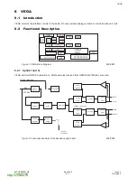
The major building blocks for the RF design are the transmit (Tx) and receive (Rx) IC’s, RF-IF dual PLL and the
antenna subsystem.
Figure 1:
RF Block Diagram
600-0301
3.2.1 Functional Description of the PLL’s
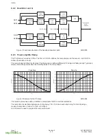
The G600 design employs two fixed IF LO’s - 201MHz for Rx and 246MHz for Tx. They are generated at 402MHz
and 496MHz using the IF part of the PLL IC. The IF VCO used is a discrete design and the VCO tuning frequency
is selectable between 402MHz and 492MHz by means of switching the frequency determining inductors,
L302+L303, by IFLOSEL control line.
The RF LO is generated by the PLL formed by the RF part of the PLL IC MB15F02 and an external modular VCO.
The use of a modular VCO improves the design repeatability.
3.2.2 Antenna
The antenna is a fixed helical type. A whip antenna may be connected to the RF path and provides better gain and
minimizes the head effects on the antenna.
The I/O connector incorporates a mechanical RF switch which routes the RF signal to the I/O connector for
handsfree operation and test purposes.
3.2.3 Transmit and Receive
The transmit and receive paths of G600 are covered in their own specific chapters later in this manual.
MCUK980101G8
Section 3
Issue 1
Technical Guide
3 - 1
Revision 0
RF OVERVIEW
Rx
201MHz
(1136.2- 1160.8)MHz
(935.2- 959.8)MHz
IF VCO
RF VCO
Tx
(890.2- 914.8)MHz
2nd LO
Rx /Tx
switch
I, Q modulation inputs
from baseband
2
2
402MHz for Rx
492MHz for Tx
I, Q outputs to baseband
zero IF


