background image

– 4-4 –

 Blocking: 

Measurement Conditions:

Wanted carrier is 3 dB above reference sensitivity.

Interferer is CW.

Spurious response exceptions:

Six exceptions are permitted IN band 915 MHz - 980 MHz.

24 exceptions are permitted OUTSIDE band 915 MHz - 980 MHz.

 Intermodulation Characteristics 

Small MS level in dB

µ

Vemf( )

Frequency

E-GSM 900

GSM 1800

FR 

±

 600 kHz to FR 

±

 800 kHz

FR 

±

 800 kHz to FR

±

 1.6 MHz

FR 

±

 1.6 MHz to FR 

±

 3 MHz

915 MHz to FR - 3 MHz 

FR 

±

 3 MHz to FR 980 MHz

FR 

±

 600 KHz to FR 

±

 800 KHz

1785 MHz to FR -  3 MHz

835 MHz to < 915 MHz

> 980 MHz to 1000 MHz

100 kHz to < 835 MHz

> 1000 MHz to 12.75 GHz

100 kHz to 1705 MHz

> 1705 MHz to < 1785 MHz

> 1920 MHz to 1980 MHz

> 1980 MHz to 12.75 GHz

70

70

80

90

90

113

113

90

90

70

70

80

87

87

113

101

101

90

Interferer Level ( f1 & f2) dBm

Interferer Frequencies ( f1 & f2 )

–49

Wanted frequency= 2f1 - f2, and [ f1 - f2] = 800 kHz

Содержание EB-VS3

Страница 1: ...0 915MHz 1710 1785 MHz 1850 1910 MHz Rx Frequency Range 925 960 MHz 1805 1880 MHz 1930 1990 MHz Tx Rx separation 10 4 MHz 20 4 MHz 20 4 MHz RF Channel Bandwidth 200 kHz Number of RF channels 174 374 299 Speech coding Full rate Half rate Enhanced Full rate Operating temperature 10 C to 55 C Type Class 4 Handheld Class 1 Handheld Class 1 Handheld RF Output Power 2 W maximum 1 W maximum 1 W maximum M...

Страница 2: ...anual should be addressed to Panasonic Mobile Communications Co Ltd 600 Saedo cho Tsuzuki ku Yokohama 224 8539 Japan CONTENTS VOL 1 1 INTRODUCTION 1 1 1 1 Purpose of the Manual 1 1 1 2 Structure of the Manual 1 1 1 3 Servicing Responsibilities 1 1 2 GENERAL DESCRIPTION 2 1 2 1 General 2 1 2 2 Features 2 1 2 3 Handportable Main Kits 2 1 3 OPERATING INSTRUCTIONS 3 1 3 1 General 3 1 3 2 Phone Overvie...

Страница 3: ...tion 9 4 9 4 Data Overwrite Procedure 9 8 9 5 VCTCXO Frequency Calibration 9 10 9 6 Transmit Power Calibration 9 12 9 7 Rxlev Calibration 9 18 VOL 5 10 REPLACEMENT PARTS LIST 10 1 10 1 Upper Unit 10 1 10 2 Lower Unit 10 2 10 3 Main PCB 10 3 10 4 Upper PCB 10 6 10 5 SIM PCB 10 8 VOL 6 11 BLOCK DIAGRAM 11 1 10 1 Baseband 11 1 10 2 RF Band 11 2 12 CIRCUIT DIAGRAM 12 1 12 1 Main PCB Baseband 12 1 12 2...

Страница 4: ...ducts powered by electricity should be serviced or repaired only by experienced professional technicians Any attempt to service or repair the product or products dealt with in this service information by anyone else could result in serious injury or death WARNING 1 INTRODUCTION 1 1 1 1 Purpose of the Manual 1 1 1 2 Structure of the Manual 1 1 1 3 Service Responsibilities 1 1 2 GENERAL DESCRIPTION ...

Страница 5: ...ne system operating on GSM Digital Cellular Networks 1 2 Structure of the Manual 1 3 Servicing Responsibilities The manual is structured to provide service engineering personnel with the following information and procedures 1 General and technical information provides a basic understanding of the equipment kits and options together with detailed information for each of the major component parts 2 ...

Страница 6: ...Rate Half Rate and Enhanced Full Rate EFR Speech Codec Triple Band E GSM 900 DCS 1800 and PCS 1900 operation Tegic T9 Text Entry Voice Ringer Desktop handsfree function comprising integral echo cancellation and noise suppression Wireless Application Protocol WAP Browser Backup Battery Downloadable polyphonic melody ring tones Clock Calculator and Currency Converter 2 3 Handportable Main Kit Figure...

Страница 7: ...INSTRUCTIONS 3 2 Phone Overview Right Soft Key Navigation Key Main Display Earpiece Silent Mode Key Power Enter Key Microphone Left Soft Key Send key Key One Push Auto Open Button Charging Indicator Camera lens Self portrait Mirror Side up Key Infrared Port Side down Key Desktop Handsfree DTHF Speaker Indicator light Multi Function Key Macro Mode Switch Personal Handsfree Connector Charging Connec...

Страница 8: ...call Return to standby mode Enter numbers and characters Press and hold 2 9 for Numeric keys Speed dialling Press and hold 0 to enter the international to prefix Asterisk key Enter In text entry mode press to change the letter case or press and hold to change the input method Enter Press and hold to switch the Silent mode on off Silent Mode key While entering a phone number press and hold to enter...

Страница 9: ...in menu Open Browser i o 4 5 Open shortcut menu Open Call log Alert mute Keyguard on Dial your voice mailbox to Speed dial Silent mode on off Switch to phone mode i Increase the volume o Decrease the volume Start stop sound recording Switch between hold and unhold on one call or switch between one active and one held call Select Menu Select Menu Select Menu Select Menu ...

Страница 10: ...rea Battery charge level Battery is charging GPRS is active Silent profile is active Meeting profile is active Outdoor profile is active Car profile is active SMS message storage area is full MMS message storage area is full Java is suspended Unread SMS message Unread MMS message Unread WAP Push message Call diverts is on Infrared is active USB connection is available New voicemail received All to...

Страница 11: ... Call Voicemail Set Mailbox number Settings Information Contacts Contacts list Phone SIM Add contact Call log Speed Dial list View groups Camera Tools Alarms Sound recorder Calculator My Media Messages Phone settings Profiles Language Time and date Illuminations Key settings Master reset Display Settings Sounds alerts Calls Connectivity Security Wallpaper Themes Brightness Backlight time Operator ...

Страница 12: ...to 1800 60 Output RF Spectrum due to Modulation Offset from Centre Frequency kHz Offset from Centre Frequency kHz Maximum Level Relative to Carrier dB Maximum Level dBm Output RF Spectrum due to Switching Transients E GSM 900 GSM 1800 400 19 22 600 21 24 1200 21 24 1800 24 27 Measurement conditions for output RF spectrum measurements Frequency Span 0 Hz Measurement Bandwidth 30 kHz Video Bandwidth...

Страница 13: ...36 36 500 MHz to 1 GHz 0 to 1MHz 100 kHz 300KHz 36 36 1 GHz to 12 75 GHz Excl relevant TX band E GSM 880 MHz to 915 MHz DCS 1710 MHz to 1785 MHz and the Rx bands 925 MHz 960 MHz 1805 MHz 1880 MHz 0 to 10 MHz 10 MHz 30 MHz offset from edge of relevant Tx band 100 kHz 300 kHz 3 MHz 300 kHz 1 MHz 3 MHz 30 30 30 30 1 0 GHz 1 710 GHz 36 1 710 GHz 1 785GHz 30 1 785 GHz 12 75GHz Relevant TX band E GSM 88...

Страница 14: ...ondition but must remain the same for FER and class 1b RBER measurements for the same channel condition Channels Propagation Conditions TU high Propagation Conditions RA Propagation Conditions HT Static Conditions Test Limit error rate Minimum No of samples Test Limit error rate Minimum No of samples Test Limit error rate Minimum No of samples Test Limit error rate Minimum No of samples TCH FS FER...

Страница 15: ...ency E GSM 900 GSM 1800 FR 600 kHz to FR 800 kHz FR 800 kHz to FR 1 6 MHz FR 1 6 MHz to FR 3 MHz 915 MHz to FR 3 MHz FR 3 MHz to FR 980 MHz FR 600 KHz to FR 800 KHz 1785 MHz to FR 3 MHz 835 MHz to 915 MHz 980 MHz to 1000 MHz 100 kHz to 835 MHz 1000 MHz to 12 75 GHz 100 kHz to 1705 MHz 1705 MHz to 1785 MHz 1920 MHz to 1980 MHz 1980 MHz to 12 75 GHz 70 70 80 90 90 113 113 90 90 70 70 80 87 87 113 10...

Страница 16: ... for use by the general public It does not contain warnings or cautions to advise non technical individuals of potential dangers in attempting to service a product Products powered by electricity should be serviced or repaired only by experienced professional technicians Any attempt to service or repair the product or products dealt with in this service information by anyone else could result in s...

Страница 17: ...ions to advise non technical individuals of potential dangers in attempting to service a product Products powered by electricity should be serviced or repaired only by experienced professional technicians Any attempt to service or repair the product or products dealt with in this service information by anyone else could result in serious injury or death WARNING 6 DISASSEMBLY REASSEMBLY INSTRUCTION...

Страница 18: ... common ground point Wrist Strap A QUICK RELEASE SKIN CONTACT DEVICE WITH A FLEXIBLE CORD WHICH HAS AN INTEGRAL SAFETY RESISTOR OF BETWEEN 5 2 kΩ AND 1 2 MΩ SHALL BE USED Containers All containers and storage must be of the conductive type WARNING The equipment described in this manual contains polarised capacitors utilising liquid electrolyte These devices are entirely safe provided that neither ...

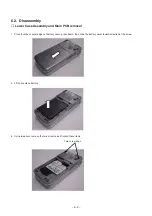
Страница 19: ... and Main PCB removal 1 Place thumbs at outer edges of battery cover press down then slide the battery cover toward direction of the arrow 2 Lift and remove battery 3 Using tweezers remove the two screw caps Discard these items Two screw caps ...

Страница 20: ...ve the four case screws Retain the screws for re use 5 Separate the two halves of the lower case assembly using a plastic strip of Guitar pick thichness as shown 6 Remove the SIM Speaker board by finger 6 3 Four case screws SIM Speaker PCB ...

Страница 21: ...rts for reassembly 8 Carefully insert tweezers into the gap between FPC and Main PCB 9 Gently lift up the tweezers direction of the arrow and then remove the FPC connector 10 Remove Main PCB from the lower front cover Note Take care not to damage the FPC connector when disconnecting the FPC from the Main PCB 6 4 Hindge holder Three panels FPC connector Upper Case Assembly and Display Modle removal...

Страница 22: ...iver to remove the four screws Retain the screws for re assembly 4 Set the phone into the Close position 5 Use a strip of plastic of guitar pick thickness to separate the case halves 6 Remove upper case assembly 6 5 Four screws ...

Страница 23: ...phone to the Open position 8 Using a small screw driver or tweezers apply presure to the one push hinge direction while pulling the hinge away from the case 6 6 9 Lift and remove the case assembly One push hinge ...

Страница 24: ... Caution Lift up open or push down close flex lock crefully If damaged a new connector must be placed on PCB 6 7 4 Release the four hooks and then remove LCD module 3 Peel the the adhesive tape and them remove the Upper PCB LCD Removal Four hooks ZIF connector Upper PCB Adhesive tape ...

Страница 25: ...ON IF ANY RF BLUETOOTH OR BASEBAND SHIELDS ARE REMOVED FROM THE PCB AT ANY TIME THEY MUST BE REPLACED WITH NEW ITEMS ONCE REMOVED THE SHIELDS MUST NOT BE REUSED Notes If the case assemblies have been disassembled and reassembled more than three times they should be replaced with new items Examine all case and cover parts before assembly If any scratches or defects are found in their finish they sh...

Страница 26: ...upper cover Assemble the Upper Cover with the Upper Case Assembly Close the four snaps making sure that both assemblies are connected 7 Fit the four screws saved during disassembly and tighten to 1 3 kgf 8 Fit two new screw covers and Main LCD panel on the Upper Cover 6 9 Screw cover Upper Case Assembly Upper Cover Macro Mode Switch Four screws LCD panel ...

Страница 27: ...cover Caution Damage to the flex circuit portion of the upper flex PCB is not repairble The flex circuit may be easily damaged during this operation causing a small tear which can grow with use and render the circuit unusable 11 Set the phone into the Open position 12 Insert the one push hinge into the lower front cover 6 10 13 Set the phone into the Close position 14 Place the hinge holder in the...

Страница 28: ...B 6 11 18 Place the lower back case on the lower front cover Fit the lower front cover to the lower back case Close the four snaps making sure that both halves are connected 19 Refit the four screws saved during disassembly 20 Tighten the upper two screws to 2 9 kgf cm and the lower two screws to 3 2 kgf cm 3 2 kgh cm 2 9 kgh cm ...

Страница 29: ... Moisture Absorbency The ALIVH PCB is more absorbent than a conventional PCB because of the nature of its material Its aramid substrate is hydrophilic i e it absorbs moisture from the air If after having absorbed moisture the ALIVH PCB is submitted to re flow or repair process moisture in the board can suddenly evaporate and cause vapour explosion Copper Foil Peel Strength Land Detachment Resistan...

Страница 30: ...plash at temperatures above 600 C 1100 F Re flowing Re touching 1 Re touching by soldering iron HAKKO 928 soldering iron is recommended 900S T B tip for thicker solder joints and 900M T LB tip for thinner solder joints are recommended 2 Tip temperature time Normal pad 325 10 C less than five seconds Large Pad 400 10 C less than five seconds 3 Pressure at solder tip 8 Weight of soldering iron 50gm ...

Страница 31: ...ernal test equipment It is required for RF calibration The following spares item is available for the PCB Repair Jig 8 RF Probe Part No MS 147 HRMJ 1 A cable with SMA female connector is provided to make the RF connection An SMA to N Type male adaptor will be required to connect the Repair Jig to the service equipment Cable losses for the RF connection are as follows A replacement RF Probe for the...

Страница 32: ... 3WZ001130AAA Dummy Battery with RF Test Jig Part No 3WZ001169AAA The power cable provides the necessary connections between the PCB repair jig dummy battery and external power supply Figure 5 3 Power Cable Figure 5 2 Dummy Battery with RF Test Jig Jig Data Cable Part No 3WZ001166AAA The Jig Data Cable is used for software download and calibration ...

Страница 33: ...de power baseband calibration and unit testing Calibrated Torque Screwdriver This screwdriver is required to secure the case screws on the phone It must have settings for 1 3 kgf and 2 5 kgf GSM Test Set This unit acts as a base station providing all the necessary GSM signalling requirements and also provides GSM signal measuring facilities ...

Страница 34: ...s in attempting to service a product Products powered by electricity should be serviced or repaired only by experienced professional technicians Any attempt to service or repair the product or products dealt with in this service information by anyone else could result in serious injury or death WARNING 8 SOFTWARE DOWNLOAD 8 1 8 1 Flash Tool update and operation guide 8 1 8 2 Installation of the Fl...

Страница 35: ...ip and progsm zip files to an appropriate directory on the hard disk of the PC e g C sw tools NOTE The progsm zip archive contains the FLS DEP and FFS files for the handset 2 In the folder where FlashTool_Release_PMC_VS3_20030625 was installed double click SETUP EXE The Setup Wizard will start serial port Stabilized Power Supply Voltage 3 7 V Headset Jack Phone PC with Dongle NOTE If using a batte...

Страница 36: ... then displayed When read click Next 3 A notice is displayed warning the user to close down all other Windows applications Close any open programs and then click Next 5 Flash Downloader will be installed under this folder by default ...

Страница 37: ... 8 3 6 Click install button ...

Страница 38: ...tton Then installation of the Dongle driver will start automatically 7 The following screen is displayed 8 Click Install button Note This driver is for using USB cable 10 Select the language preference Then click OK button ...

Страница 39: ... 8 5 11 Click Next button Then installation will start ...

Страница 40: ... is powerd OFF 4 Short press the power key of handset Note Do not press hold the power key If the handset powers on please retry from step 3 If PC has recoginized the device as CDC please CANCEL the installation and disconnect the USB cable from the handset Detach attach the battery them re try from step 3 12 Click Finish button 5 Click Next button ...

Страница 41: ... 8 7 6 Following screen will be appeared 7 Click Continue Anyway button 8 Click Finish button ...

Страница 42: ...shTool FlashTool_6_1 in PC menu Then the following screen apperas Click the tab of Use SPK file Select SPK file The following screen is displayed Click None If you have specifine spk file before the file name is displayed to specify Spk file as shown in the following procedure Click None ...

Страница 43: ...lect spk file and press Open button Then the path and name of spk file are displayed Then Click OK Check that all required files are in the same folder COM port set up The following screen is displayed Move to the folder where diffs is located ...

Страница 44: ...sation The download procedure is as follows 1 Ensure that fully charged battery is connected to the phone 2 Connect the handest to the PC via the date cable Click around Click to start Press the power button on handset After the above procedure download starts CAUTION Should the PC or Download application crash or lock up during downloading calibration data in the phone may be lost To minimise the...

Страница 45: ... 8 11 When download starts progress bar is displayed Do not disconnect the date cable while downloading When download is successful the following screen is displayed ...

Страница 46: ...se of an error the following screen is displayed If a download fails check all connect ions between the phone data cable and PC Before restarting the download procedure remove and then re attach the phone battery ...

Страница 47: ...accurate to 0 2 dB MUST be used The output power of the phone can be influenced by the RF Logic shield covers therefore all power calibration procedures MUST be performed with the shield frames and covers fitted IF ANY OF THE RF OR LOGIC SHIELDS ARE REMOVED FROM THE PCB AT ANY TIME THEY MUST BE REPLACED WITH NEW ITEMS ONCE REMOVED THE SHIELDS MUST NOT REUSED Tx Calibration can be performed manuall...

Страница 48: ... 50 15 12 50 13 00 13 50 16 10 50 11 00 11 50 17 8 50 9 00 9 50 18 6 50 7 00 7 50 19 4 50 5 00 5 50 Power Level PL Output Power dBm Min Max Target Nominal 0 29 00 29 25 29 50 1 27 75 28 00 28 25 2 25 50 26 00 26 50 3 23 50 24 00 24 50 4 21 50 22 00 22 50 5 19 50 20 00 20 50 6 17 50 18 00 18 50 7 15 50 16 00 16 50 8 13 50 14 00 14 50 9 11 50 12 00 12 50 10 9 50 10 00 10 50 11 7 50 8 00 8 50 12 5 50...

Страница 49: ...24 50 4 21 50 22 00 22 50 5 19 50 20 00 20 50 6 17 50 18 00 18 50 7 15 50 16 00 16 50 8 13 50 14 00 14 50 9 11 50 12 00 12 50 10 9 50 10 00 10 50 11 7 50 8 00 8 50 12 5 50 6 00 6 50 13 3 50 4 00 4 50 14 1 50 2 00 2 50 15 0 50 0 00 0 50 Power Level PL Output Power dBm Min Max Target Nominal ...

Страница 50: ... Test Mode Press the key and key at the same time and then turn on the power key of the mobile phone Start the PhoneTool program The following screen is then displayed With Dongle PC PCB Repair Jig PS 1 DC Power supply Jig Data Cable 3 7V T Key and Key Turn on power ...

Страница 51: ... click Set 1 Click the V24 AT On and check the log window AT OK 2 Click the Update Info button and check the log window OK Note If the massage ERROR is displayed check the cable connections the power supply and that the phone is switched on Repeat step1 and 2 With Dongle PC PCB Repair Jig PS 1 DC Power supply Jig Data Cable 4 2 V and 3 2 V T ...

Страница 52: ...iled 9 Enter the average vbat ADC into the VS3_ADC_Cal Excel sheet in the vbat 4 2 V field 10 Change the power supply voltage from 4 2 V to 3 2 V If this average value is outside the range of 3138 to 3503 then the unit has failed 11 Enter the average vbat ADC into the VS3_ADC_Cal Excel sheet in the vbat 3 2 V field 12 Change the power supply voltage from 3 2 V to 3 7 V for Calibration for Confirma...

Страница 53: ...eld The recorded VBAT TBAT value will be used to automatically calculate the VBAT_ GAIN OFFSET and TBAT_GAIN OFFSET It will then be stored to the eep file of the BATT format Excel sheet With Dongle PC PCB Repair Jig PS 1 DC Power supply Jig Data Cable 3 7 V T PS 2 DC Power supply 1 8 V 0 for Calibration for Confirmation TBAT 1 8 TBAT 0 0 Gain Offset adc value cal value 3951 2039 64 2039 OK OK OK O...

Страница 54: ...k Read EEPROM value from the phone The eep static folder is opened 3 Click Load Eeprom Text File for Calibration for Confirmation I 0 8 A I 0 2 A Gain Offset adc value cal value 3795 2461 1253 2016 OK OK OK OK 907 8 Convert the Excel sheet of EEP data to TXT text format 9 File Save As Text Tab delimited Save 10 Rename the epp file from the original filename and then save to PC 037A eep_static chr_...

Страница 55: ...select which is saved VS3_ADC_ Cal text Tab delimited file from PC 6 Select Text file and then click Open 7 Click Download current Eeprom value to phone 8 Click OVERWRITE button The VS3_ADC_Calibration values in the phone will be overwritten by the new values from the PC ...

Страница 56: ...AT OK 2 Click the Update Info button and check the log window OK 3 Click mode button and select Backlight 4 Set the LCD type to Main 5 Set Action to Off and then click to Set 6 Set Action and Fade to Off and then click Set 9 5 VCTCXO Frequency Calibration ...

Страница 57: ...ode This enables the transmitter Check that a Tx signal is seen on the GSM Test Unit Measure the frequency error A calibrated VCTCXO should provide a frequency error within 800 Hz at room temperature 9 The frequency and therefore the VCTCXO is adjusted by charging the AFC DAC value in PhoneTool Adjust the AFC DAC value until the frequency error measured on the GSM Test Set is within 800 Hz Note th...

Страница 58: ... GMSK Mode 4 Before starting Power Level Calibration the Power Ramp Editor should be enabled The Power Ramp Editor popup window is displayed 9 6 Transmit Power Calibration To begin calibration of the transmitter select Non signaling Test from the Modes pull down menu in PhoneTool and complete the following steps ...

Страница 59: ... heading check the TX The handset will transmit and the power meter will displayed the default Tx power output 7 Input an appropriate value for DAC16 and Check that the power mater registers a change in power level Note Before setting a new DAC16 value turn off the transmitter by clicking RF Mode Off DAC 16 value Calibration Channels The following table shows calibration channels It is important t...

Страница 60: ...utomatically calculate the channel compensation value and it in the appropriate eep memory location on the eep worksheet within the same Excel file GSM DCS PCS PL dac PL dac PL dac 5 1142 0 1140 0 1116 6 1009 1 977 1 944 7 956 2 920 2 887 8 851 3 813 3 779 9 759 4 719 4 687 10 676 5 639 5 607 11 604 6 568 6 538 12 541 7 505 7 478 13 486 8 450 8 424 14 437 9 401 9 378 15 394 10 357 10 338 16 355 11...

Страница 61: ...CC eep_static gmsk_rf_comp gmsk_pa_ch_comp 1 11 2 0 09CE eep_static gmsk_rf_comp gmsk_pa_ch_comp 1 11 3 0 09D0 eep_static gmsk_rf_comp gmsk_pa_ch_comp 1 12 0 0 09D2 eep_static gmsk_rf_comp gmsk_pa_ch_comp 1 12 1 0 09D4 eep_static gmsk_rf_comp gmsk_pa_ch_comp 1 12 2 0 09D6 eep_static gmsk_rf_comp gmsk_pa_ch_comp 1 12 3 0 09D8 eep_static gmsk_rf_comp gmsk_pa_ch_comp 1 13 0 0 5 1142 1142 0 6 1009 100...

Страница 62: ...rget power is listed in the Nominal column The calibrated power must always fall within the Target Min and Max ranges listed to the right of the Nominal target PL Target Output Power Level dBm 5 32 00 32 25 32 50 6 29 20 29 45 29 70 7 27 90 28 15 28 40 8 26 75 27 00 27 25 9 24 50 25 00 25 50 10 22 50 23 00 23 50 11 20 50 21 00 21 50 12 18 50 19 00 19 50 13 16 50 17 00 17 50 14 14 50 15 00 15 50 15...

Страница 63: ... Click Read EEPROM value from the phone The eep static folder is opened 3 Click Load Eeprom Text File 4 Select Any File of the Files of type 5 Click Lock in and then select which is saved VS3_GSMK_0ffset_ Cal text Tab delimited file from PC 6 Select Text file and then click Open ...

Страница 64: ... 9 18 7 Click Download current Eeprom value to phone 8 Click OVERWRITE button The S3_GSMK_0ffset_ Cal values in the phone will be overwritten by the new values ...

Страница 65: ...into the RX Excel sheet below The IQRMS value will be used to calculate the gain and channel compensation values It will then stored to the eep file of the RX Excel sheet 9 Repeat steps 1 through 8 for all calibration channels 10 When all channels and bands are calibrated save the Excel sheet of eep data using File Save As Text Tab delimited Save 9 7 Rxlev Calibration For RX Level calibration the ...

Страница 66: ..._gain_comp 1 6 1 0281 eep_static rf_adjcomp rxlev_gain_comp 1 7 1 0282 eep_static rf_adjcomp rxlev_gain_comp 1 8 1 0283 eep_static rf_adjcomp rxlev_gain_comp 1 9 1 0284 eep_static rf_adjcomp rxlev_gain_comp 1 10 1 027A eep_static rf_adjcomp rxlev_gain_comp 1 0 1 027B eep_static rf_adjcomp rxlev_gain_comp 1 1 1 027C eep_static rf_adjcomp rxlev_gain_comp 1 2 1 027D eep_static rf_adjcomp rxlev_gain_c...

Страница 67: ...e from the phone The eep static folder is opened 3 Click Load Eeprom Text File Data Overwrite Procedure 4 Select Any File of the Files of type 5 Click Lock in and then select which is saved VS3_Rxlevel_ Cal text Tab delimited file from PC 6 Select Text file and then click Open ...

Страница 68: ...7 Click Download current Eeprom value to phone 8 Click OVERWRITE button The VS3_RxLeve_ Cal values in the phone will be overwritten by the new values from the PC 8 7 9 22 ...

Страница 69: ... public It does not contain warnings or cautions to advise non technical individuals of potential dangers in attempting to service a product Products powered by electricity should be serviced or repaired only by experienced professional technicians Any attempt to service or repair the product or products dealt with in this service information by anyone else could result in serious injury or death ...

Страница 70: ...1108AAA CAMERA PANEL M014 3CH001350AAA LENS HOLDER M015 3CV001779AAA CAMERA CUSHION M016 3CH001351AAA CAMERA SHIELD LOWER M017 3CH001352AAA CAMERA SHIELD UPPER M018 3DJ001262AAA CAMERA MACRO SWITCH M019 3CF002719AAC SCREW SHEET SILVER 3CF002719AAE SCREW SHEET BLACK M020 3AB001165AAA CHANGEABLE SCREW M021 3AB001160AAA UPPER CASE SCREW M022 3DH001599AAA CAN SHIELD IC M023 3DH001600AAA CAN SHIELD DC ...

Страница 71: ... PLATE M058 3CJ001292AAA NAME PLATE SHEET M059 3CH001354AAA SIM PCB HOLDER M060 3AB001154AAA LOWER SCREW M061 3DB001114AAB SCREW CAP GRAY 3DB001114AAC SCREW CAP BLACK M062 3DH001602AAA SHIELD LOGIC L COVER M063 3DH001603AAA SHIELD LOGIC L FRAME M064 3DH001604AAA SHIELD LOGIC S COVER M065 3DH001605AAA SHIELD LOGIC S FRAME M066 3DH001606AAA SHIELD RF COVER M067 3DH001607AAA SHIELD RF FRAME M068 3DJ0...

Страница 72: ...C CAPACITOR 330 pF 25V C524 F1L0J333A019 CERAMIC CAPACITOR 0 033 uF 6 3V C525 F1J1C1050031 CERAMIC CAPACITOR 1 uF 16V C526 F1G1A104A012 CERAMIC CAPACITOR 0 1 uF 10V C527 F1G1A104A012 CERAMIC CAPACITOR 0 1 uF 10V C528 ECJZEB1E102K CERAMIC CAPACITOR 0 001 uF 25V C529 F1G0J1050007 CERAMIC CAPACITOR 1 uF 6 3 V C531 F1G0J1050007 CERAMIC CAPACITOR 1 uF 6 3 V C550 ECJ0EC1H470J CERAMIC CAPACITOR 47 pF 50V...

Страница 73: ...NECTOR CN504 K1KB50A00116 50PIN SOCKET CN505 K1MZ05A00003 5PIN BATTERY CONNECTOR D101 B0BC7R4A0015 DIODE D501 B0BD6R800011 DIODE D505 B0BC7R4A0015 DIODE D506 MAZW068H0L DIODE D507 MA2S72800L DIODE D612 MAZW068H0L DIODE D613 MAZW068H0L DIODE D614 MAZW068H0L DIODE D615 MAZW068H0L DIODE D616 MAZW068H0L DIODE D617 MAZW068H0L DIODE D618 B0BC7R4A0015 DIODE D901 B0JCMD000023 DIODE D902 B0JCPB000001 DIODE...

Страница 74: ...J2GE0R00X FIXED RESISTOR 0 Ohm 1 16W R594 ERJ1GEJ103C FIXED RESISTOR 10K Ohm 1 20W R600 ERJ2GEJ4R7X FIXED RESISTOR 4 7 Ohm 1 16W R601 ERJ2GEJ332X FIXED RESISTOR 3 3K Ohm 1 16W R602 ERJ2GEJ220X FIXED RESISTOR 22 Ohm 1 16W R604 ERJ2RKF3002X FIXED RESISTOR 30K Ohm 1 16W R605 ERJ2GEJ220X FIXED RESISTOR 22 Ohm 1 16W R606 ERJ2GE0R00X FIXED RESISTOR 0 Ohm 1 16W R607 ERJ1GE0R00C FIXED RESISTOR 0 Ohm 1 20W...

Страница 75: ...3AZB0000028 LED FL3001 J0JCC0000249 FILTER FL3002 EXC24CP221U FILTER FL3003 J0HAAA000024 FILTER FL3004 J0HAAA000024 FILTER FL3006 J0HAAA000016 FILTER FL3007 J0HAAA000016 FILTER FL3008 J0HAAA000016 FILTER FL3009 J0HAAA000016 FILTER FL3010 J0HAAA000016 FILTER FL3011 J0HAAA000021 FILTER L3001 G1A220CA0007 COIL 22UH L3002 G1A4R7EA0012 COIL 4 7UH Q3006 UNR921MJ0L TRANSISTOR Q3007 B1GFCFEN0005 TRANSISTO...

Страница 76: ...TOR 0 1 uF 10 V C705 ECJ0EC1H180J CERAMIC CAPACITOR 18 pF 50 V CN701 K1KA14A00255 14PIN CONNECTOR CN702 K1NA06E00008 6PIN SIMCARD CONNECTOR D701 MAZS0750ML DIODE FL701 EXC24CP221U FILTER 5 V 350MA R701 ERJ2GE0R00X FIXED RESISTOR 0 Ohm 1 16W RV701 D4ED18R00004 VARISTOR 33 pF 8 V RV702 D4ED18R00004 VARISTOR 33 pF 8 V RV703 D4ED12700002 VARISTOR 27 V RV704 D4ED12700002 VARISTOR 27 V RV705 D4ED18R0000...

Страница 77: ...mpting to service a product Products powered by electricity should be serviced or repaired only by experienced professional technicians Any attempt to service or repair the product or products dealt with in this service information by anyone else could result in serious injury or death WARNING 11 BLOCK DIAGRAMS 11 1 11 1 Baseband 11 1 11 2 Power Source 11 2 12 CIRCUIT DIAGRAMS 12 1 12 1 Main PCB L...

Страница 78: ...IN LCD TMDT TFT 2 2 QVGA MELODY HS AMP KEYPAD 7 x 7 SPEAKER MIC HSJ RECEIVER I2C SERIAL DIF IQ AND IF C ONTROL IrDA INTERFACE Demultiplexedd 16 bit parallel data bus GPIO x 3 SIM INTERFACE 7 x 7 RGB 0 17 VIBRATOR EL KEY BACKLIGHT BATTERY Li Ion CHARGER Backup Battery DIRECT USB ON THE GO IF USART POWER AMP 1 ANTENNA SWITCH 1 ANTENNA CURRENT MONITOR DC DC LCD BACKLIGHT YUV I2C 16 BIT 16 BIT 16 BIT ...

Страница 79: ...er Gauss Filter 1 2 1 4 SigmaDelta MASH Modulator Fif0 Frac CW Int CW Cntrl RX TX Cntrl 3 Wire Bus MMD Timing Measurement VCO Control CLG Adjust Fast RFD Fast CP DAO AFC BUFEN BUFOUT B BX A AX VCO Bias Voltage Regulator TX Bias BSW Driver LF Balun Balun VBATT HBT U101 Transceiver FL203 FL202 FL201 U103 Antenna Switch Module U102 PA Module U105 U106 U401 TCXO Module Power controller ...

Страница 80: ...C18 SSC2_SCLK C17 SSC2_MRST C16 VSS_MAIN_1 C15 T_OUT1 C14 T_OUT0 C13 I2S3_CLK C12 I2S3_TX C11 T_OUT4 C10 T_OUT5 C9 RF_DATA C7 VSS_DSP_2 H7 VSSP_EBU_RING_2_3_2 H8 VSSP_DIG_D1 H9 VSSP_DIG_CENTRE H9 H10 VSSP_DIG_CENTRE H10 H11 VSSP_DIG_CENTRE H11 H12 VSSP_DIG_B H13 VDD_DSP_1 H14 VDD_MAIN_1 H15 VDDP_DIG_A2 H19 PAD_PAOUT1 O H20 PAD_BB_IX B H21 PAD_BB_Q B J1 EBU_A 16 J2 EBU_A 17 J3 EBU_A 10 J7 VDDP_EBU_...

Страница 81: ... 1 BS 2 VCC1A 3 DCS PCS_IN 4 GSM_IN 5 GND 5 6 VCC1B 7 GND 7 8 GND 8 9 GND 9 10 GND 10 11 GSM_OUT 12 GND 12 13 GND 13 14 GND 14 15 DCS PCS_OUT 16 GND 16 17 VBATT 18 ENABLE 19 RSVD GND 21 GND_PAD 1 GND 1 2 GSM850 GSM900 TX 3 GND 3 4 PCS RX 5 DCS RX 6 GND_OR_N C 6 7 GSM850 GSM900 RX 8 VC3 9 GND_OR_N C 9 10 VC1 11 GND 11 12 ANTENNA 13 GND 13 14 VC2 15 GND 15 16 DCS PCS TX 17 GND 17 18 GND 18 19 GND 19...

Страница 82: ...1 L2 AB4 L1 FPCS1 K15 CNF2 K14 FPSCK K13 FPDAT7 K12 AB5 K4 AB2 K3 AB3 K2 AB8 K1 FPDAT17 J15 CNF1 J14 FPA0 J13 FPDAT16 J12 VSS J4 J4 AB6 J3 AB7 J2 AB9 J1 PIO1VDD H15 H15 VSS H14 H14 FPDAT14 H13 CNF7 H12 GPIO10 F13 FPDAT11 F12 DB4 F4 DB3 F3 HIOVDD F2 F2 DB5 F1 FPDAT10 E15 GPIO7 E14 COREVDD E13 E13 GPIO9 E12 VSS E4 E4 SI E3 DB6 E2 SCS E1 CM1DAT1 D10 CM1HREF D9 PLLVDD D8 CM2HREF D7 VSS D6 D6 CM2DAT4 D...

Страница 83: ...SET VINT PWM1 GND GND DIF_CLK GND GND VBAT GND GND GND RECN GND VBB2 VBAT DIF_MRST NC GND DIF_CS RECP VBAT GND GND 2V85 GND GND VBAT 2V85 VBB2 V_SD VINT VBB2 V_SD VINT VBAT 2V85 E47 16 49 47 E39 E44 E18 E34 11 E29 51 6 31 7 19 29 E14 40 30 E22 E13 E6 E43 E41 E19 E3 48 13 E4 27 E50 E17 44 E40 E35 E11 33 E26 E5 45 E42 50 43 E20 4 E25 10 E21 22 E37 E12 E8 17 18 E24 E28 28 E33 23 15 52 24 8 E1 E49 12 ...

Страница 84: ... SPOUT2 NC NC SPEAKER CN702 SIM CN 1 2 3 4 5 6 E701 E702 FL701 1 2 3 4 RV703 RV704 D701 RV701 RV702 RV705 C704 0 1U C702 0 1U C705 18p C701 2 2U C703 0 1U R701 0 RV706 16 10 6 11 CN701 7 14 8 1 2 12 13 9 3 15 5 4 SIM_CLK SIM_IO SIM_RST V_SIM SPOUT1 SPOUT2 ...

Страница 85: ...18 TP616 TP615 TP904 TP905 R545 560 TP908 RV501 R1047 100 100 R1048 TP906 DS1008 DS1006 S113 S115 S118 S125 S128 S120 S121 S109 S110 S105 S106 S111 S107 S101 S103 S112 S108 S104 S102 S127 S123 RV503 R504 390K RV502 C580 C579 RV508 R604 30K C610 0 1U C620 0 1U C630 0 1U C576 0 1U C577 0 1U C584 C573 C572 C581 R606 0 C606 0 1U RV1001 D612 DS1009 DS1010 D617 D614 D615 D613 100 100 100 100 100 100 R10...

Страница 86: ...01 U103 D903 CN502 DS1016 U105 U106 D1002 Q1001 BT900 CN504 CN102 FL602 FL601 U903 R1053 R1054 R1055 C504 0 33U C556 0 1U C509 C401 0 01U C408 0 01U C406 C124 0 1U C616 0 1U C603 0 1U C607 0 1U C563 0 1U C524 0 1U C522 0 1U C523 0 1U C604 0 1U C605 0 1U C560 10p C562 10p C505 22U 4V C506 22U 4V C614 0 1U C612 0 1U 0 0 C658 0 1U C657 0 1U C586 0 1U C587 0 1U R583 100K R584 100K R550 R661 R660 R553 ...

Страница 87: ... 3 Upper PCB Upper Side 13 3 TP3011 TP3008 TP3022 TP3023 TP3029 TP3030 TP3017 TP3031 TP3014 TP3010 TP3009 TP3007 TP3021 TP3003 TP3001 TP3005 TP3027 TP3025 TP3026 TP3028 TP3015 TP3020 TP3002 TP3006 TP3012 ...

Страница 88: ...3007 FL3008 FL3010 FL3009 FL3006 R3074 R3007 C3060 C3059 R3006 R3009 R3010 R3089 RV3005 RV3004 RV3003 DS3002 47 U3005 Q3008 1 5K 1 5K L3001 22UH U3002 D3001 1K C3067 C3024 C3025 0 1U 0 1U 1U 1U 47p CN3003 CN3001 CN3002 0 0 L3002 4 7UH U3004 1U 1U C3019 C3018 C3088 C3050 FL3002 C3047 C3048 C3046 U3009 Q3007 Q3006 C3087 R3060 C3001 0 1U 0 1U 0 1U 0 1U 0 1U 0 1U 10K 0 1U 0 1U 0 1U 0 1U 0 1U C3015 C30...

Страница 89: ... 13 5 13 5 FPC PCB CN1 ...

Страница 90: ... 13 6 13 6 SIM PCB C703 C702 RV705 C701 C705 2 2U FL701 RV702 R701 0 18p RV706 RV703 RV701 D701 CN701 E701 E702 0 1U 0 1U 0 1U C704 RV704 CN702 ...

Отзывы: